The Microchip: How Two Men Independently Shrank a Room
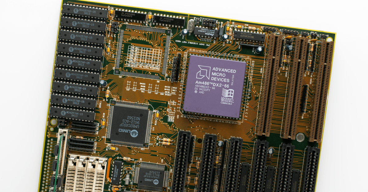
Photo: Nicolas Foster / Pexels
In the summer of 1958, Jack Kilby was the newest hire at Texas Instruments — so new that he had no vacation time, so he stayed in the lab while everyone else left for August. Alone with a bench full of germanium and a notebook, he sketched out an idea that would eventually pack more than 92 billion transistors into a chip smaller than a fingernail. Six months later and 1,500 miles northwest, Robert Noyce independently arrived at a cleaner version of the same idea. Neither man knew the other was working on it. Both were right.
The Problem That Made the Microchip Necessary
By the mid-1950s, electronics had hit a wall. The U.S. military's most advanced guided missiles required thousands of individual components — resistors, capacitors, transistors — each hand-soldered onto a circuit board with hair-thin wires. The more complex the system, the more wires, and the more wires, the more failures. The Air Force calculated that its most advanced computers were breaking down faster than they could be repaired.
Tyranny of numbers — the phrase engineers used for this era. You could make any individual component more reliable, but multiply unreliability across ten thousand components and the system still failed constantly. The math was brutal: even if each component worked 99.99% of the time, a circuit with 10,000 of them had only a 37% chance of working at all.
Source: IEEE History Center (2000) — documented in Jack Kilby's Nobel Prize lecture, December 2000.
The obvious solution — connect all those components on a single piece of semiconductor material — was considered impractical. If you could make a transistor from silicon, why not also make the resistors and capacitors from silicon? The resistance of the material itself could serve as a resistor. The geometry of the layers could act as a capacitor. Everything from one block of semiconductor, no wires required.
The idea was obvious enough that several engineers had thought of it. The problem was that nobody believed the resulting components would be good enough to use.
The Story Behind the Discovery
Jack St. Clair Kilby arrived at Texas Instruments in May 1958 with a background in ceramic materials and a restless curiosity about miniaturization. When the lab emptied for the summer break, he had no holiday allowance and the run of the facility.
By July he had filled a notebook with calculations. On September 12, 1958, he demonstrated the first working integrated circuit to TI management: a germanium sliver roughly 7 mm long, with a single transistor and a handful of passive components embedded in the same piece of material. The connections were made with gold wire, hand-bonded under a microscope. It was crude. It worked.
Source: Texas Instruments corporate history archive; also Kilby's Nobel Prize lecture, NobelPrize.org (2000).
The demonstration was deliberately modest. Kilby powered the circuit and showed that it produced a continuous sine wave on an oscilloscope. His supervisor, Willis Adcock, reportedly said: "That's not very impressive." Kilby replied: "No, but it's monolithic."
Meanwhile, at Fairchild Semiconductor in Mountain View, California, Robert Noyce was working toward the same destination by a different route. Noyce had access to a new manufacturing technique invented by his colleague Jean Hoerni: the planar process. Instead of building up components on a bumpy, three-dimensional surface, Hoerni's method kept everything flat — planar — by oxidizing the top of a silicon wafer and etching away layers with acid and light.
In January 1959, Noyce wrote in his lab notebook the key insight: you could evaporate aluminum directly onto the silicon surface to form the connecting wires, eliminating hand-bonded gold wire entirely. His integrated circuit was made of silicon (not germanium), used the planar process, and could actually be manufactured reliably in quantity.
Source: Invention of the Integrated Circuit, Wikipedia; Robert Noyce entry, Computer History Museum.
| Date | Event |
|---|---|
| September 12, 1958 | Kilby demonstrates first working IC at Texas Instruments |
| January 23, 1959 | Noyce writes the planar IC concept in his lab notebook |
| February 6, 1959 | Kilby files patent for "miniaturized electronic circuits" |
| April 25, 1961 | Noyce's planar IC patent granted (filed July 1959) |
| 1966 | Kilby and Noyce share the IEEE Medal of Honor |
| 1990 | Noyce dies of a heart attack, age 62 |
| October 10, 2000 | Kilby awarded Nobel Prize in Physics |
How It Actually Works
An integrated circuit is, at its core, a map of logic printed onto silicon. The trick is that silicon is a semiconductor — it conducts electricity under some conditions but not others, and that conditional behavior is exactly what you need to build a switch.
Transistor — a three-terminal semiconductor device that acts as an electrically controlled switch or amplifier. When voltage is applied to the gate (the control terminal), current can flow between the source and drain terminals. No voltage, no current. That's your "0" and "1."
A modern integrated circuit layers transistors, interconnects, and insulators through a process called photolithography. Imagine printing a newspaper, but instead of ink on paper, you're using light to etch patterns into silicon coated with a light-sensitive chemical (called a photoresist), then washing away the exposed parts with acid, depositing metal to fill the gaps, and repeating the process dozens of times to build up layer after layer of circuitry.
The analogy that holds up: photolithography is like printing, except instead of one layer of ink, you print 80 to 100 layers precisely aligned on top of each other, each layer defining a different part of the circuit, at tolerances measured in fractions of an atom.
Source: TSMC Technology Overview (2024); Intel Fabrication Technology Background.
What Kilby proved was that you could integrate components. What Noyce proved was that you could manufacture the result. Both insights were necessary. Kilby's version could be built in a lab; Noyce's could be built in a factory.
Why Silicon Beat Germanium
Kilby used germanium because it was what TI worked with. Noyce used silicon because Fairchild's planar process worked better on it. The choice mattered: germanium stops working reliably above about 70°C (158°F), making it unsuitable for most real-world applications. Silicon remains stable up to roughly 150°C (302°F) and is, conveniently, the second most abundant element in Earth's crust. Silicon won.
Source: Semiconductor materials comparison, IEEE Spectrum historical archive.
From Millimeters to Nanometers
The first IC Kilby demonstrated had components measured in millimeters. By 1971, Intel's 4004 processor — the first commercially available microprocessor — packed 2,300 transistors onto a 10mm² chip using a 10-micrometer (10,000 nm) process. By 2025, TSMC's production 3nm chips contain over 100 billion transistors, and its 2nm process was entering commercial production with a further 10–15% performance improvement over 3nm.
Source: TSMC Technology Roadmap (2024); Intel 4004 historical documentation, Intel Museum.
That compression — from 10,000 nanometers to 2 nanometers in roughly 50 years — is what Moore's Law describes.
The People Involved
Jack Kilby (1923–2005)
Kilby grew up in Great Bend, Kansas, the son of a utility company manager. He earned a degree in electrical engineering from the University of Illinois in 1947 and spent a decade at Centralab in Milwaukee before joining Texas Instruments. He was quiet, methodical, and — by his own description — someone who liked to solve problems by working backward from what was physically possible, not forward from what was theoretically elegant.
After the IC, Kilby went on to co-invent the handheld calculator (TI's Cal-Tech prototype, 1967) and the thermal printer. He spent his final decades as a distinguished professor at Texas A&M. When the Nobel Committee called in 2000, he was reportedly out for his morning walk. He died in 2005, age 81.
Source: Jack Kilby Nobel Prize biography, NobelPrize.org (2000).
Robert Noyce (1927–1990)
Noyce was Kilby's photographic negative as a personality: charismatic, visionary, and comfortable in a room full of people who needed convincing. He grew up in Grinnell, Iowa, the son of a Congregationalist minister, and earned his PhD in physics from MIT in 1953. His gift was translating engineering into business.
Noyce was one of the eight engineers who left William Shockley's laboratory in 1957 to found Fairchild Semiconductor — a group that William Shockley himself bitterly called "the traitorous eight." A decade later, Noyce and Gordon Moore left Fairchild to found Intel. If Kilby invented the IC, Noyce built the industry that manufactured it.
He died of a heart attack on June 3, 1990, age 62, too early for the Nobel Prize Committee. When Kilby accepted his prize in Stockholm in 2000, he told the assembled audience that Noyce "deserved to share" the honor.
Source: Robert Noyce biography, Computer History Museum; Traitorous Eight, Wikipedia.
Gordon Moore and the Law He Named
Gordon Moore co-founded Intel with Noyce in 1968. In 1965, while still at Fairchild, he published a paper in Electronics magazine observing that the number of components per integrated circuit had doubled every year since 1958, and predicting this would continue for "at least" ten more years. In 1975 he revised the doubling period to two years. His observation — now known as Moore's Law — held roughly true for five decades before physical limits began slowing it down around 2010.
Source: Gordon Moore, "Cramming More Components onto Integrated Circuits," Electronics, April 19, 1965.
The Patent and Priority Disputes
The patent battle between TI and Fairchild lasted a decade. Both companies filed patent applications in 1959: Kilby in February, Noyce in July. The Patent Office initially awarded the key interconnection patent to Noyce, reasoning that his planar metal connections were the truly novel contribution. TI appealed. The Court of Customs and Patent Appeals reversed and awarded a patent to Kilby in 1969 — a decade after the invention.
The resolution was anticlimactic: TI and Fairchild (by then owned by Schlumberger) agreed in 1966 to cross-license their respective patents to each other rather than continue litigating. The practical effect was that both companies could manufacture ICs without paying the other, and both received royalties from the rest of the industry. The legal settlement explicitly avoided declaring a sole inventor.
Source: DPMA (German Patent Office), "65 Years of the Integrated Circuit" (2023); Allaboutcircuits.com historical analysis.
The academic community has largely reached a pragmatic consensus: Kilby demonstrated first, Noyce designed better. Both are credited as co-inventors. The Nobel Committee, forced to choose, gave the prize to Kilby because Noyce was no longer alive — Nobel Prizes are not awarded posthumously.
A third claim occasionally surfaces: the British engineer Geoffrey Dummer published a paper in 1952 describing a solid-state circuit with no connecting wires — conceptually identical to the IC. Dummer never built a working prototype, and his proposal predates the planar process that made manufacture possible. His claim is historically interesting but technically incomplete.
The Traitorous Eight and Silicon Valley
The story of the integrated circuit cannot be separated from the story of how eight engineers walked out on a Nobel laureate and, in doing so, invented an entire geography.
William Shockley had won the 1956 Nobel Prize in Physics for co-inventing the transistor. He moved to Mountain View, California, to be near his aging mother and founded Shockley Semiconductor Laboratory. He recruited some of the most talented young physicists in the country. Then he managed them so badly — with personality testing, lie detectors, and relentless second-guessing — that eight of them mutinied together.
The eight: Julius Blank, Victor Grinich, Jean Hoerni, Eugene Kleiner, Jay Last, Gordon Moore, Robert Noyce, and Sheldon Roberts. In September 1957, they approached Fairchild Camera and Instrument for backing, and Fairchild Semiconductor was born with $1.5 million in funding.
Source: Traitorous Eight, Wikipedia; Allaboutcircuits.com, "The Traitorous Eight and the Rise of Fairchild Semiconductor."
From Fairchild, the diaspora spread across the Santa Clara Valley. Noyce and Moore founded Intel in 1968. Jerry Sanders, who had left Fairchild slightly later, founded Advanced Micro Devices (AMD) in 1969. By one estimate, more than 400 companies trace their founding lineage back to Fairchild. The term "Silicon Valley" — coined by journalist Don Hoefler in 1971 — would not exist without the Traitorous Eight.
Source: Fairchild Semiconductor, Britannica Money; AMD founding history, AMD corporate archives.
Unintended Consequences
The Calculator and the End of Human Arithmetic
Kilby's integrated circuit work at TI led directly to the handheld calculator. The TI Cal-Tech prototype (1967) was the first device to perform calculations using a single IC. The commercial successor, the Pocketronic, went on sale in Japan in 1970. By the late 1970s, the $20 scientific calculator had eliminated the job of "computer" — human beings, overwhelmingly women, who spent careers doing long multiplication for engineering firms and insurance companies.
The Weapon Inside Everything
The impetus for the integrated circuit was military — specifically, the need to fit complex guidance electronics into missiles and spacecraft. The first major customer for TI's ICs was the U.S. Air Force's Minuteman II missile program. By 1962, every Minuteman II carried 22 ICs. The revenue from this contract funded the development of the consumer IC market.
Source: Chiphistory.org, "Integrated Circuit Invention and History 1958."
Environmental Costs Nobody Predicted
Silicon fabrication requires ultrapure water in quantities that strain regional water supplies. A single TSMC fab in Taiwan uses roughly 156,000 tonnes of water per day. The photolithography process also uses dozens of exotic chemicals — many carcinogenic — that require careful disposal. The hidden environmental cost of the device in your pocket runs to thousands of liters of water and grams of rare earth elements per chip.
Source: TSMC Environmental Social Governance Report (2023).
Where the Microchip Stands Today
Kilby's 1958 IC had one transistor. Modern chips have billions. The journey from one to one hundred billion in 65 years is the fastest sustained pace of miniaturization in the history of technology.
TSMC began production of 3nm chips in 2022 and is bringing 2nm to volume production in 2025, manufactured at its Hsinchu Science Park facility in Taiwan. At 2nm, features on the chip are smaller than a strand of DNA (roughly 2.5 nm diameter). Gate-all-around (GAA) nanosheet transistors — which surround the channel on all four sides rather than three — are replacing the FinFET design that powered the previous decade of scaling.
Source: TSMC Technology Roadmap (2024); IEEE Spectrum, "TSMC 2nm Process" (2024).
The frontier is now three-dimensional. Rather than making transistors smaller, chipmakers are stacking dies on top of each other (3D IC integration), connecting layers with copper pillars called through-silicon vias (TSVs). NVIDIA's Blackwell B100 GPU, with approximately 208 billion transistors and built on a multi-die architecture, is the current transistor-count record holder for a commercially available device.
Source: NVIDIA Blackwell architecture white paper (2024).
The limiting factor going forward is not physics but economics: a state-of-the-art 2nm fab costs approximately $20 billion to build. Only three companies in the world — TSMC, Samsung, and Intel — have the capital and technical expertise to operate at the leading edge. The microchip, which began as a solution to the problem of too many wires, is now the most strategically contested physical object on Earth.
For a deeper look at the device that made the IC possible in the first place, see The Transistor.
What People Get Wrong About the Microchip
The most common misconception is that Kilby and Noyce were racing each other. They were not. Neither knew the other was working on the problem. The parallel invention happened because both were responding to the same documented military need with the same materials that had become available in the mid-1950s. Independent co-invention of this kind is common in the history of science precisely because the state of knowledge at any given moment makes certain solutions newly obvious to anyone paying close attention.
A second misconception: that Moore's Law is a law of physics. It is not. It is an empirical observation and, for decades, a self-fulfilling prophecy — because the semiconductor industry used it as a planning target, companies invested to meet it, and it kept holding. Since roughly 2010, transistor density growth has slowed below the two-year doubling rate. Moore's Law hasn't been repealed; it has been revised into a slower exponential, sustained by 3D stacking and new transistor geometries rather than simple planar shrinkage.
Source: Physics World, "Moore's Law: Further Progress Will Push Hard on the Boundaries of Physics and Economics" (2023).
A third error: crediting Silicon Valley's rise entirely to Stanford University or the 1950s military-industrial complex. Both were necessary conditions. The sufficient condition was eight engineers who couldn't stand their boss and had the nerve to leave together.
Frequently Asked Questions
Q: Who actually invented the microchip — Kilby or Noyce? A: Both. Kilby demonstrated the first working integrated circuit on September 12, 1958, using germanium. Noyce independently designed a silicon-based version using the planar process in January 1959, which was more manufacturable. The U.S. Patent Office awarded patents to both; TI and Fairchild cross-licensed in 1966 rather than litigate. Kilby received the 2000 Nobel Prize because Noyce had died in 1990 and the Nobel is not awarded posthumously.
Q: What is the difference between an integrated circuit and a microchip? A: They are the same thing. "Integrated circuit" (IC) is the technical term — a circuit in which all components are fabricated on a single piece of semiconductor material. "Microchip" or "chip" is the informal name used in press and everyday speech. "Microprocessor" is a specific type of IC that contains the logic unit, arithmetic unit, and control functions of a computer processor on one chip.
Q: Why is silicon used instead of other materials? A: Silicon combines several practical advantages: it forms a stable oxide (SiO₂) that works as an excellent insulator and etch mask; it is mechanically strong; it remains a reliable semiconductor up to about 150°C; and it is the second most abundant element in Earth's crust, making it cheap. Newer materials like gallium nitride (GaN) and silicon carbide (SiC) outperform silicon in specific high-power or high-frequency applications, but silicon dominates general computing because of its mature manufacturing ecosystem.
Q: What is Moore's Law and is it still holding? A: Gordon Moore observed in 1965 that the number of transistors per integrated circuit was doubling roughly every year, and revised this to every two years in 1975. Transistor counts have continued to rise, but the doubling period has stretched to roughly three years since 2010, and the improvements come increasingly from architectural changes (3D stacking, new transistor geometries) rather than straightforward planar shrinkage. The "law" continues to serve as an industry roadmap, but it is no longer as predictive as it was in 1975–2010.
Q: How many transistors are in today's best chips? A: As of 2025, NVIDIA's Blackwell B100 GPU contains approximately 208 billion transistors, the highest count in a commercially available chip. TSMC's 2nm process, entering volume production in 2025, packs roughly 1 trillion transistors per square centimeter at maximum theoretical density.
Q: Why does it matter that TSMC makes chips in Taiwan? A: TSMC produces the majority of the world's leading-edge semiconductor logic chips. Because advanced semiconductor fabrication requires a dense ecosystem of specialized suppliers, equipment makers, and trained engineers built up over decades, production cannot easily be moved. Roughly 90% of chips at 10nm or below are manufactured in Taiwan, making the island a single point of failure for the global electronics supply chain — a geopolitical dependency that governments worldwide are now spending billions to reduce.
Q: What is a "nanometer" in the context of chips? A: The "nm" in chip process nodes (2nm, 3nm, 7nm) originally referred to the physical gate length of a transistor. In modern usage, the number is essentially a marketing label for a generation of manufacturing technology — the actual smallest feature may be somewhat larger or smaller than the named process node. At 2nm, individual features are smaller than a strand of DNA, which has a diameter of about 2.5nm.
Read next:
Follow new articles
Add SciHub101 to your feed reader to see new science and technology stories.
About the Author
SciHub101 is an independent science and technology publication founded and edited by Buğra Sözeri, a software engineer and app developer based in Türkiye. AI tools assist with drafting and research. Source documentation in the existing archive is uneven, and articles are being reviewed and corrected. The Editorial Team byline identifies editorial responsibility; it does not certify specialist or independent human review. Where we compare products, anything built by our own team is labelled as such — see the editorial guidelines and About page for how corrections and disclosures work.
Related Articles
The Invention of the Microscope
From Zacharias Janssen's first compound microscope around 1590 to Nobel-winning super-resolution techniques: how the microscope revealed the hidden universe of cells and microbes.

The Invention of the Laser
How Townes and Schawlow's 1958 paper, Maiman's 1960 ruby device, and a 30-year patent war produced the most versatile tool in modern science.
Microchip Invention: Kilby, Noyce, and the Integrated Circuit
The microchip emerged from parallel breakthroughs by Jack Kilby and Robert Noyce. This guide explains the invention that made modern computing possible.
The Personal Computer: From Kit to Commodity
How the Altair 8800, Apple I, and IBM PC turned computing from an institution's tool into a personal one — and why IBM's open architecture was its biggest strategic blunder.

The Invention of the Transistor
How three physicists at Bell Labs in 1947 built a device smaller than a paperclip that would become the foundation of every computer ever made.

Countries with the Most Venture Capital Investment (2025 Ranked)
The United States attracts over $150 billion in venture capital annually — more than the rest of the world combined. China is a distant second. Israel is the world's highest VC-to-GDP ratio nation. Here's the full venture capital ranking — and why the geography of startup funding determines where tomorrow's industries are built.