How Semiconductor Fabs Work
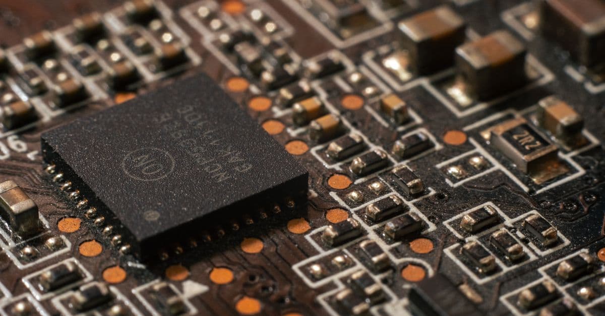
Photo: Ivan Chumak / Pexels
A semiconductor fab is a factory that turns a blank disc of ultra-pure silicon into a chip carrying billions of transistors, using hundreds of sequential steps of patterning, deposition, etching, doping, cleaning, and inspection. Building one modern logic chip can take more than 1,000 individual process steps and roughly three months from raw wafer to finished die (TSMC, 2024). This guide walks through what actually happens inside the building, why it costs tens of billions of dollars to open one, and why so few companies on Earth can do it at all.
What a fab actually is
A fab, short for fabrication facility, is not one machine. It is hundreds of specialized machines arranged in a loop, connected by an automated material handling system that shuttles wafers between them in sealed pods so human hands never touch the silicon directly. The entire building is built around one requirement: keep dust, vibration, and chemical drift low enough that features a few nanometers wide survive intact through hundreds of process passes.
That requirement is why a leading-edge fab costs so much to build in the first place. Intel's Ohio fab project and TSMC's Arizona expansion have each carried price tags in the tens of billions of dollars, and industry analysts put a single advanced logic fab at $20 billion or more once tools, cleanroom construction, and utilities are included (SEMI, 2024). Most of that money does not go into the building shell. It goes into the tools sitting inside it — a single extreme ultraviolet (EUV) lithography machine from the Dutch company ASML costs $150–$200 million on its own, and a modern fab needs dozens of different tool types working in a precise sequence (Tom's Hardware, 2026).
The wafers themselves start as boules of monocrystalline silicon grown by the Czochralski process, in which a seed crystal is dipped into molten silicon and slowly pulled upward while rotating, producing a cylindrical ingot that is later sliced into thin discs. Those discs, typically 300 millimeters (about 12 inches) in diameter for modern fabs, are polished to near-atomic flatness before they ever enter a process tool. A defect invisible to the naked eye at this stage can wipe out every chip built on top of it later, which is why the entire building exists to prevent exactly that kind of error.
The cleanroom — why air itself is a manufacturing input
Every fab is built around a cleanroom, a sealed environment where filtered air is pushed downward through the ceiling and pulled out through a perforated floor at a rate of dozens of air changes per hour. Workers wear full-body "bunny suits" that cover skin, hair, and breath, not for their own protection but for the wafer's. A human shedding roughly 100,000 skin flakes per hour is, from a fab's perspective, a walking contamination source.
Cleanliness is measured in ISO 14644 classes, which count particles of a given size per cubic meter of air. Most leading-edge fabs run their most sensitive process bays — where lithography and etch happen — at ISO Class 1 to 3, while less critical areas run at Class 4 to 6, which still allows only 352 to 35,200 particles of 0.5 micrometers or larger per cubic meter (TSI, 2026). For comparison, ordinary outdoor air contains millions of such particles per cubic meter. High-Efficiency Particulate Air (HEPA) filters catch 99.97 percent of particles at 0.3 micrometers, but the newest fab bays increasingly rely on Ultra-Low Penetration Air (ULPA) filters, which catch 99.999 percent of particles at 0.12 micrometers, because sub-10-nanometer transistor features cannot tolerate even trace airborne contamination.
Humidity control matters just as much as particle count. Photoresist, the light-sensitive chemical coating used to pattern circuits, absorbs moisture and can warp if relative humidity drifts outside a tight band; operators who let humidity swing beyond about five percentage points have reported defect densities climbing by as much as 50 percent (Dersion Clean, 2026). Think of the cleanroom less like a room and more like a chemistry lab shrunk down to the scale of individual atoms, where the "equipment" includes the air itself.
Why can't a fab just be built anywhere?
Vibration is the other invisible enemy. Lithography tools position features with sub-nanometer precision, so fabs are built on massive vibration-isolated foundations, away from rail lines, highways, and even ocean waves where possible. TSMC's Taiwan fabs and Intel's Oregon campus both sit on engineered slabs designed to damp out ground movement that would otherwise blur a printed circuit line.
Photolithography — printing a circuit with light
Lithography is the step that defines a chip's geometry, and it works by projecting a pattern through a mask onto a wafer coated with photoresist, then developing that pattern the way a photograph is developed. A tool called a stepper or scanner moves the wafer beneath a lens system, exposing one small section — called a die site — at a time, then stepping to the next, repeating the exposure dozens of times across a single 300-millimeter wafer.
For decades, fabs used deep ultraviolet (DUV) light at a 193-nanometer wavelength, often combined with a thin film of water between the lens and the wafer (immersion lithography) to bend the light further and sharpen the pattern. That technique carried the industry from roughly the 65-nanometer node down to about 7 nanometers. Below that, features became smaller than the wavelength of light being used to print them, which is where extreme ultraviolet (EUV) lithography — light with a 13.5-nanometer wavelength, produced by vaporizing microscopic droplets of molten tin with a laser 50,000 times a second — became necessary (ASML, 2026).
ASML is the sole commercial maker of EUV lithography systems in the world, which makes the company a structural chokepoint in the entire semiconductor supply chain. Each EUV scanner contains components sourced from more than 5,000 suppliers across two dozen countries, and the mirrors inside it are polished so precisely that if one were scaled up to the size of Germany, its tallest imperfection would be under a millimeter (ASML, 2026). In 2026, ASML began shipping its next-generation High-NA EUV systems, and Intel became the first chipmaker to put a High-NA-produced logic chip into production, while TSMC has signaled it will likely wait until its 1-nanometer-class "A10" node, expected around 2029–2030, before adopting the more expensive High-NA tools at volume (SemiAnalysis, reported by Chip Stock Investor, 2026). Samsung, by contrast, has committed to using High-NA EUV for its 2-nanometer SF2 process in 2026, illustrating how the three leading foundries are now taking genuinely different technology bets rather than following one shared roadmap.
How many times does a wafer pass through lithography?
A single advanced logic chip requires 60 to 100 or more separate lithography exposures across its full manufacturing flow, because each layer of metal wiring and each transistor structure needs its own pattern. Every one of those passes must align to the previous layer within a few nanometers, which is why lithography alone can account for a third or more of total fab processing time.
Etching, deposition, and doping — building the transistor stack
Lithography only creates a pattern in photoresist; it does not cut or build anything by itself. Etching is the step that removes material through the openings in that pattern, either with reactive chemical baths (wet etching) or, far more commonly at advanced nodes, with an ionized gas called plasma that bombards the wafer in a vacuum chamber (dry or plasma etching). Plasma etching can cut features with near-vertical sidewalls at nanometer precision, which is essential once transistor structures move from flat, two-dimensional shapes to the three-dimensional fin and gate-all-around designs used at nodes below about 22 nanometers.
Deposition does the opposite job: it adds thin films of material, atom by atom or molecule by molecule, using techniques such as chemical vapor deposition (CVD), physical vapor deposition (PVD), and atomic layer deposition (ALD). ALD in particular can lay down a film one atomic layer at a time, giving engineers control over film thickness to within a fraction of a nanometer — a level of precision that would have sounded absurd to chipmakers in the 1990s but is now routine for the gate dielectrics and metal barriers inside a modern transistor.
Doping introduces controlled impurities into specific regions of the silicon to change how it conducts electricity, creating the positively and negatively charged regions that make a transistor switch on and off. Ion implantation, in which dopant atoms such as boron or phosphorus are accelerated by an electric field and fired into the wafer, is the dominant technique today because it allows precise control over both the concentration and depth of the dopant. After implantation, wafers pass through rapid thermal annealing, a brief, intense heating step that repairs the crystal damage caused by the implant and activates the dopant atoms electrically.
These three steps — etch, deposit, dope — repeat in varying combinations, layer after layer, as the chip is built upward from the silicon substrate. A modern logic chip can have 15 or more layers of interconnect metal wiring stacked above the transistors themselves, each one requiring its own lithography, etch, and deposition sequence. That is the real source of the "hundreds of steps" figure often quoted for advanced chips: it is not hundreds of different techniques, but the same handful of techniques applied over and over with extreme precision at every layer.
Inspection, metrology, and the yield problem
Every few process steps, wafers are pulled aside for inspection and metrology, the measurement of feature dimensions, film thickness, and alignment accuracy. Optical and electron-beam inspection tools scan for particle defects, pattern bridging, and misalignment, while scatterometry and other non-contact measurement techniques verify that critical dimensions stay within a tolerance often measured in single-digit nanometers.
This matters because of yield, the percentage of chips on a wafer that function correctly at the end of the line. Yield is inversely related to defect density: contamination or misalignment introduced early in the process compounds across every subsequent layer, so a defect rate that sounds small at any one step can produce a meaningfully lower yield by the time a chip has passed through a thousand steps. Foundries treat mature-node yield figures above roughly 90 percent as commercially healthy, while brand-new leading-edge nodes often start well below that and climb over months of production tuning — which is one reason a new process node typically launches on lower-volume, higher-margin chips before it reaches mainstream products.
Why do new chip nodes get expensive and scarce right after launch?
New nodes launch with lower yield because engineers are still tuning hundreds of interacting process variables simultaneously. Foundries allocate early low-yield capacity to customers who can absorb higher per-chip cost, such as premium smartphone processors, while yield improves before the node reaches high-volume, cost-sensitive products.
Why the industry is so concentrated
Only a handful of companies on Earth can run a leading-edge logic fab at all: TSMC, Samsung, and Intel, with TSMC alone handling the large majority of the world's most advanced logic chip production for external customers (fabless designers such as Apple, Nvidia, and AMD, who design chips but do not manufacture them). That concentration is not accidental. Building a competitive fab requires simultaneous mastery of materials science, optics, chemistry, robotics, and software, backed by tens of billions of dollars of capital and a supply chain that itself has no redundancy — ASML's EUV monopoly being the clearest example.
This is also why geopolitics and chip manufacturing have become inseparable topics. A large share of the world's most advanced logic capacity sits in Taiwan, which is why governments in the United States, European Union, Japan, and elsewhere have committed billions of dollars in subsidies through programs such as the US CHIPS and Science Act to encourage fab construction on their own soil. Fabs being built under those programs still depend on the same handful of equipment suppliers and the same specialized engineering talent pool, so geographic diversification is happening, but slowly, and the industry's fundamental structure — a small number of tool makers feeding a small number of foundries — is not changing quickly.
The history behind that structure traces back to a single event: the invention of the point-contact transistor at Bell Labs on December 16, 1947, by John Bardeen, Walter Brattain, and William Shockley, work that earned the three the 1956 Nobel Prize in Physics (Computer History Museum; Nokia Bell Labs, 2026). Every fab described in this article exists to mass-produce, with atomic precision, an idea that started as a slab of germanium and two gold contacts on a lab bench.
What people get wrong about fabs
A common misconception is that a "3-nanometer" or "2-nanometer" chip has transistor features that are literally 3 or 2 nanometers wide. In practice, node names are now marketing labels tied loosely to transistor density and performance rather than a single measured dimension; the actual gate structures on a "3nm" chip are typically closer to 12–15 nanometers in some dimensions, even as other features shrink well below that (industry analysis, 2026). The number is useful for comparing generations within one company's roadmap, but it is not a literal ruler measurement anyone can verify with calipers.
Another misconception is that building a new fab is mostly a construction project. The building itself, floor space, power, and water systems are a real engineering challenge, but the tooling budget dwarfs the construction budget at the leading edge. A company can spend years securing enough EUV scanner allocation from ASML alone before a fab can even begin producing at volume, because ASML's own production capacity — roughly 65 low-NA EUV systems planned per year as of 2026, expanding further in 2027 — is itself a bottleneck shared across every customer worldwide (Tom's Hardware, 2026).
Finally, people often assume more advanced nodes are always the goal for every chip. In reality, plenty of chips — automotive controllers, power management circuits, many sensors — are built on mature, decades-old nodes because those processes are cheaper, more reliable, and entirely adequate for the job. The 2021–2023 global chip shortage was driven in large part by shortages of these older, "trailing edge" chips, not the newest 3-nanometer parts, a detail that got lost in most of the shortage coverage at the time.
| Process step | What it does | Key tool or technique | Typical repeats per chip |
|---|---|---|---|
| Wafer prep | Grows and polishes the silicon substrate | Czochralski crystal growth, chemical-mechanical polishing | 1 (per wafer) |
| Photolithography | Prints the circuit pattern onto photoresist | DUV immersion scanner, EUV scanner | 60–100+ |
| Etching | Removes material through the patterned openings | Plasma (dry) etch, wet chemical etch | Dozens |
| Deposition | Adds thin films of conductor, insulator, or semiconductor | CVD, PVD, atomic layer deposition | Dozens |
| Doping / annealing | Alters electrical properties of specific regions | Ion implantation, rapid thermal anneal | Dozens |
| Inspection / metrology | Verifies dimensions and screens for defects | E-beam and optical inspection, scatterometry | After most steps |
| Packaging / test | Cuts wafer into dies, wires and tests each chip | Dicing saw, wire bonding or advanced packaging, automated test | 1 (per chip) |
A modern logic chip cycles through this sequence hundreds of times across roughly 1,000 total process steps before it is a finished, tested part.
The takeaway
A fab is best understood as a factory built entirely around precision and cleanliness rather than raw output, where the building, the air, and the ground itself are all engineered components of the manufacturing process. That precision is why so few companies can build one, why the ones that exist concentrate enormous geopolitical weight, and why a chip that looks identical to the naked eye can represent a fundamentally different generation of physics underneath. The transistor started as two gold contacts on a slab of germanium in 1947; the modern fab is what it takes to print 50 billion of them onto a fingernail-sized chip without a single one going wrong.
Read next:
- How GPUs Work — Why AI Needs Them
- Why Semiconductors Are So Hard to Make
- How AI Models Are Trained: The Full Process
Frequently Asked Questions
Q: What is the simplest answer to how semiconductor fabs work? A: A fab turns blank silicon wafers into chips by repeating a cycle of photolithography, etching, deposition, and doping across dozens of layers, checking dimensions and defects after nearly every step, until a finished chip contains its full transistor and wiring structure.
Q: Why do fabs need to be so clean? A: Transistor features on modern chips are only a few nanometers wide, smaller than most airborne dust particles, so a single stray particle landing during lithography or etching can ruin a chip layer. Fabs run at ISO Class 1–6 cleanliness, filtering out nearly all particles down to sub-micron sizes (TSI, 2026).
Q: Why is EUV lithography so important and so expensive? A: EUV uses 13.5-nanometer-wavelength light to print features too small for older deep ultraviolet tools to resolve. ASML is the only commercial maker of EUV scanners, each costing $150–$200 million, which makes EUV both a physics necessity and a supply-chain chokepoint for the entire industry (ASML, 2026).
Q: What does a chip's node name like "3nm" actually mean? A: It no longer refers to a single physical measurement. Node names are now roughly comparative labels for a generation's transistor density and performance; actual feature sizes on a "3nm" chip vary by dimension and are often larger than 3 nanometers in practice.
Q: Why does chip manufacturing depend so heavily on a few companies? A: Leading-edge fabs require tens of billions of dollars of capital, decades of accumulated process expertise, and equipment from suppliers like ASML that have no real competitors. That combination limits the number of companies that can operate at the cutting edge to essentially TSMC, Samsung, and Intel.
Q: What should I read next? A: See related SciHub101 explainers on how GPUs work and why AI needs them, why semiconductors are so hard to make, and how AI models are trained.
Sources
- ASML, "EUV Lithography Systems," company product documentation, 2026.
- Tom's Hardware, "ASML's roadmap for chipmaking lithography tools examined — from DUV to Low-NA, High-NA, Hyper-NA, and beyond," 2026.
- TechTimes, "ASML Raises Full-Year Guidance as Intel Ships First High-NA EUV Logic Chip," July 2026.
- Chip Stock Investor / SemiAnalysis, "TSMC Announces New Manufacturing Nodes Through 2029 — but No ASML High-NA EUV," 2026.
- TSI Incorporated, "Meet ISO 14644 Cleanroom Standards," 2026.
- Angstrom Technology, "What Are Semiconductor Cleanrooms?," 2026.
- Dersion Clean, "Semiconductor Cleanroom Requirements: A Guide to ISO Classes, AMC & ESD Control," 2026.
- Computer History Museum, "1947: Invention of the Point-Contact Transistor," The Silicon Engine.
- Nokia Bell Labs, "1956 Nobel Prize in Physics," bell-labs history archive, 2026.
- SEMI, industry capital expenditure reporting on advanced fab construction costs, 2024.
Follow new articles
Add SciHub101 to your feed reader to see new science and technology stories.
About the Author
SciHub101 is an independent science and technology publication founded and edited by Buğra Sözeri, a software engineer and app developer based in Türkiye. AI tools assist with drafting and research. Source documentation in the existing archive is uneven, and articles are being reviewed and corrected. The Editorial Team byline identifies editorial responsibility; it does not certify specialist or independent human review. Where we compare products, anything built by our own team is labelled as such — see the editorial guidelines and About page for how corrections and disclosures work.
Related Articles

Humanoid Robots Explained: Why 2026 Is a Turning Point
Humanoid robots combine AI, batteries, motors, hands, perception, and manufacturing economics. This guide explains what is real, what is hard, and where they may work first.

How Passkeys Replace Passwords
Passkeys promise phishing-resistant login without memorized passwords. This guide explains public-key cryptography, device sync, recovery, and real security tradeoffs.
EUV Lithography Explained: The Machine Behind Advanced Chips
Extreme ultraviolet lithography uses 13.5nm light from vaporized tin droplets to print the smallest chip features. Here is how ASML's machines actually work.

Why Semiconductors Are So Hard to Make — Inside the World's Most Complex Manufacturing Process
A modern chip is built from up to 100 patterned layers aligned at nanometer precision, inside cleanrooms and with machines that few companies can build. Here is why that is so hard, and why it costs so much.
Best Free E-Signature Tools in 2026 (No Signer Account)
Best free e-signature tools in 2026 where signers need no account: eSignSimple, Zoho Sign, SignWell, Dropbox Sign, DocuSign and Adobe compared on limits and audit trails.