How GPUs Work — Why AI Needs Them
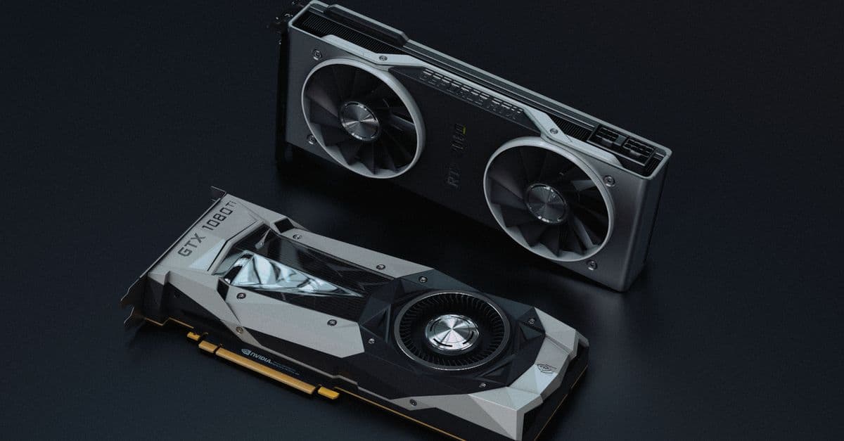
Photo: Nana Dua / Pexels
Every large AI model in use today was trained on thousands of graphics processing units, and most of the answers those models give are computed on GPUs too. That is a strange outcome for a chip designed to colour pixels in video games. The explanation comes down to one idea: parallelism. Drawing a 3D scene means doing the same small calculation for millions of pixels, and training a neural network means doing the same small calculation for billions of numbers. A chip built for the first job turned out to be well suited to the second.
This article explains how a GPU is organised, why that organisation matches the mathematics of neural networks, what tensor cores and high-bandwidth memory add, and where the real bottlenecks lie. Specifications are taken from NVIDIA's own documentation and datasheets, because NVIDIA's chips are the most widely documented; the same principles apply to AMD's Instinct accelerators and to custom AI chips. We have avoided prices and market-share figures, which change quickly and are rarely published by primary sources.
From Pixels to Parameters: A Short History
In the 1990s, 3D graphics was one of the hardest workloads a personal computer faced. Each frame of a game required transforming the corners of thousands of triangles into screen positions, computing how light falls on them, and then filling in the colour of every pixel. CPUs could not do all of that at 60 frames per second, so graphics cards took on more of the work.
In 1999, NVIDIA released the GeForce 256, which it marketed as the world's first GPU. Its main innovation was hardware transform and lighting (T&L): the geometry and lighting calculations moved from the CPU onto the graphics chip, freeing the processor and letting developers use many more polygons. Whether it was truly "the first GPU" depends on definitions, but it marked the point where the graphics chip became a processor in its own right.
The next step was programmability. In the early 2000s, graphics chips gained programmable shaders, small programs that run once for every vertex or every pixel. Researchers quickly noticed that if you disguised a scientific calculation as a shading problem, a graphics card could run it far faster than a CPU. That trick was awkward, so NVIDIA built a general-purpose programming model, CUDA, which lets programmers write ordinary C-like code for the GPU. NVIDIA's CUDA documentation carries a copyright beginning in 2007 and describes CUDA as "a parallel computing platform and programming model" used in deep learning, scientific computing and high-performance computing.
The moment that tied GPUs to AI came in 2012. Alex Krizhevsky, Ilya Sutskever and Geoffrey Hinton at the University of Toronto trained a deep convolutional neural network, later called AlexNet, on about 1.2 million ImageNet training images. The network had about 60 million parameters and 650,000 neurons. Their paper states it took "five to six days on two NVIDIA GTX 580 3GB GPUs," and explains that they split the network across two cards because "a single GTX 580 GPU has only 3GB of memory, which limits the maximum size of the networks" that could be trained. A variant of the network won the ILSVRC-2012 competition with a top-5 test error rate of 15.3%, compared with 26.2% for the second-best entry. Notice that memory, not arithmetic, was already the limiting factor. It still is.
For the neural network side of that story, see our explainer on how neural networks work.
CPU vs GPU: Two Ways to Spend Transistors
A modern processor has a fixed budget of transistors and power. CPUs and GPUs spend that budget in opposite ways.
A CPU spends a large share of its silicon on making a small number of threads run as fast as possible. It has a modest number of large cores, each with big caches, sophisticated branch prediction that guesses which way the program will go, and out-of-order execution that reorders instructions to avoid waiting. This makes CPUs excellent at tasks with lots of decisions, irregular memory access and little repetition: running an operating system, a web browser or a database query. Our article on how CPUs work goes into those mechanisms.
A GPU spends most of its silicon on arithmetic units and simply runs a huge number of threads. Rather than trying hard to make any one thread fast, it hides delays by switching between thousands of threads: when one group is waiting for memory, another group runs. This only works if the workload offers enough independent threads, but when it does, the throughput is enormous.
| Design choice | CPU | GPU |
|---|---|---|
| Number of cores | Few, large | Many, small, grouped into streaming multiprocessors (SMs) |
| Goal | Minimise the time for one thread (latency) | Maximise total work per second (throughput) |
| Handling of memory delays | Large caches, prediction, out-of-order execution | Switch to another group of threads while one waits |
| Best workloads | Branchy, irregular, sequential code | The same operation on very large arrays of data |
| Programming model | Threads, often a handful to dozens | Thousands to millions of lightweight threads |
Inside a GPU: SMs, Warps and SIMT
NVIDIA's GPUs are built from repeated blocks called streaming multiprocessors (SMs). NVIDIA's H100 in its SXM5 form has 132 SMs. Each SM contains arithmetic units, a large register file, a block of fast on-chip shared memory, and schedulers that decide which threads run each cycle.
The thread hierarchy
The CUDA programming guide describes how a program, called a kernel, is launched "with many threads, often millions of threads." Those threads are organised in three levels:
- Threads are the individual workers. Each has its own registers and usually handles one element or a small piece of the data.
- Thread blocks group threads that can cooperate. The guide states that "all threads of a thread block are executed in a single SM," which lets them share data through the SM's shared memory and synchronise.
- Grids are the full set of blocks for one kernel launch. Blocks and grids can be one-, two- or three-dimensional, which conveniently matches images, matrices and volumes.
Warps and SIMT
Inside an SM, the hardware does not schedule threads one at a time. According to the CUDA guide, "threads are organized into groups of 32 threads called warps," and "a warp executes the kernel code in a Single-Instruction Multiple-Threads (SIMT) paradigm." All 32 threads in a warp execute the same instruction at the same time, each on its own data.
SIMT has a cost. If threads in a warp take different branches of an if statement, the guide explains, the threads not on the current path are masked off while the others run, and then the roles swap. Code with lots of divergent branches therefore wastes GPU capacity. Code that applies the same operation to every element of a large array, which is exactly what neural network layers do, keeps every lane of every warp busy.
The memory hierarchy
The guide lists the main memory spaces a GPU programmer works with:
- Registers, where the register file "stores thread local variables" and are the fastest storage on the chip.
- Shared memory, which "is accessible by all threads within a thread block or cluster." On H100, NVIDIA says shared memory is configurable up to 228 KB per SM, within a combined 256 KB shared-memory and L1 cache.
- L2 cache, shared by all SMs. H100 has 50 MB of L2.
- Global memory, which the guide defines as "the DRAM attached to the GPU," accessible to all SMs. On data-centre GPUs this is high-bandwidth memory (HBM).
Moving data down this hierarchy costs time and energy at every step. Much of the art of fast GPU code, and of AI software libraries, consists of loading a tile of data from global memory into shared memory once and then reusing it as many times as possible.
Why Neural Networks Love This
A neural network layer takes a batch of inputs, multiplies them by a matrix of learned weights, adds a bias and applies a simple non-linear function. Training repeats this forward pass, then runs a backward pass that computes how each weight should change, which again consists mostly of matrix multiplications. Transformers, the architecture behind today's language models, are built from the same ingredients: their attention and feed-forward layers are dominated by large matrix products. Our guide to transformers explained simply walks through those layers.
Matrix multiplication is ideal GPU work for three reasons:
- Independence. Each element of the output matrix is a dot product of one row and one column. Every one of those dot products can be computed separately, so a large product offers millions of independent tasks.
- Regularity. The same multiply-and-add operation is applied everywhere, so warps rarely diverge.
- Reuse. Each input number is used many times. If a block of threads loads a tile of each matrix into shared memory, it can perform many operations per byte fetched, which keeps the arithmetic units fed.
A worked example
Consider multiplying two square matrices of size 4,096 × 4,096. The output has 4,096 × 4,096 ≈ 16.8 million elements. Each element needs 4,096 multiplications and 4,096 additions, so the whole product requires about 2 × 4,096³ ≈ 137 billion floating-point operations.
The inputs, stored in 16-bit format, take 2 bytes × 16.8 million ≈ 33.5 MB each, so about 67 MB must be read and 33.5 MB written, roughly 100 MB in total. That is about 1,370 operations per byte of memory traffic, if the data is reused perfectly. A workload with that much arithmetic per byte is called compute-bound: the speed of the arithmetic units sets the pace. On an H100, whose dense 16-bit tensor throughput is about 990 trillion operations per second (half of NVIDIA's 1,979 TFLOPS figure, which assumes sparsity), the arithmetic would take on the order of 0.14 milliseconds at peak. Real kernels reach a fraction of peak, but the point stands: big matrix products are where GPUs shine.
Now consider adding two large vectors element by element. Each pair of numbers is used once, for one addition. That is less than one operation per byte, so the GPU spends nearly all its time waiting for memory. Such operations are memory-bound, and they are why memory bandwidth matters so much.
Tensor Cores: Matrix Units in Hardware
Ordinary GPU arithmetic units, which NVIDIA calls CUDA cores, perform one fused multiply-add on one pair of numbers per cycle. Because AI is dominated by matrix multiplication, NVIDIA added dedicated units for it, starting with the Volta architecture and the V100 GPU in 2017.
NVIDIA's developer documentation for Volta explains that "each Tensor Core provides a 4x4x4 matrix processing array that performs the operation D = A * B + C," where A, B, C and D are small matrices. "Each Tensor Core performs 64 floating-point FMA mixed-precision operations per clock," multiplying 16-bit inputs and accumulating in higher precision. The V100 had 640 tensor cores, eight per SM, and NVIDIA quoted up to 125 tensor TFLOPS. Programmers reach these units through warp-level matrix operations in CUDA: the 32 threads of a warp cooperate on a tile, for example 16 × 16 × 16, rather than each thread working alone.
Later generations widened the formats and the throughput:
- Hopper (H100) has 528 fourth-generation tensor cores, four per SM, and a Transformer Engine that, according to NVIDIA, chooses between 8-bit floating point (FP8) and 16-bit precision layer by layer, handling the scaling automatically.
- Blackwell adds support for 4-bit floating point (FP4) using what NVIDIA calls micro-tensor scaling, which NVIDIA says "doubles the performance and size of next-generation models that memory can support."
Why lower precision helps
Every halving of number size halves the memory needed to store a value and the bandwidth needed to move it, and lets the hardware pack more multipliers into the same silicon. Neural networks tolerate this surprisingly well, because their computations are statistical: small rounding errors in individual weights mostly average out. Training typically uses 16-bit formats such as BF16 or FP16, with higher-precision accumulation, and increasingly FP8 for parts of the computation. Inference can often go lower still. Our explainer on LLM quantization covers how models are compressed to 8-bit and 4-bit integers.
Read the footnotes on peak numbers
NVIDIA's H100 datasheet lists 1,979 TFLOPS for FP16 and BF16 tensor operations and 3,958 for FP8, but marks these with a footnote: "With sparsity." That refers to a feature in which hardware skips structured zeros in a weight matrix. Without sparsity, the figures are half as large, and NVIDIA's Hopper architecture article gives dense FP16/BF16 at about 1,000 TFLOPS. Peak figures also assume perfect conditions that real workloads rarely achieve. Comparing a sparse figure for one chip with a dense figure for another is one of the most common mistakes in hardware comparisons.
Memory: The Real Bottleneck
AlexNet's authors split their model across two cards because of memory. Fourteen years later, memory capacity and bandwidth remain the main constraints on AI hardware.
Data-centre GPUs use high-bandwidth memory (HBM): stacks of DRAM dies placed right next to the GPU on the same package and connected by a very wide interface. This gives far more bandwidth than the GDDR memory on gaming cards, at higher cost.
| GPU (NVIDIA) | Memory | Memory bandwidth | Source |
|---|---|---|---|
| V100 (2017) | HBM2 (capacity varies by model) | — | NVIDIA Volta documentation |
| H100 SXM | 80 GB HBM3 | 3.35 TB/s | NVIDIA H100 datasheet |
| H200 SXM | 141 GB HBM3e | 4.8 TB/s | NVIDIA H200 product page |
Why capacity matters for large language models
A model's weights must sit in GPU memory to be used efficiently. The arithmetic is straightforward: a model with 70 billion parameters stored at 2 bytes each (16-bit) needs about 140 GB just for its weights. That exceeds a single H100's 80 GB and nearly fills an H200's 141 GB, before counting the working memory used during computation.
Training needs far more than the weights. The optimizer used for most large models, Adam, keeps two extra values per parameter, and training usually keeps a higher-precision master copy of the weights as well. Activations, the intermediate results of the forward pass, must be stored for the backward pass. Together these can multiply memory needs several times over, which is why large models are trained across many GPUs at once.
During inference, language models also keep a key-value (KV) cache: stored intermediate results for every token already processed, so that each new token does not require recomputing the whole conversation. The cache grows with the length of the context and with the number of simultaneous users. Our article on the context window explains why long contexts are expensive.
Why bandwidth matters for inference
When a language model generates text one token at a time for a single user, each new token requires reading essentially all the model's weights from memory, but performs only a couple of operations per weight. That is a memory-bound workload. A rough upper bound on speed is memory bandwidth divided by model size: an H100 reading 140 GB of weights at 3.35 TB/s could manage at most about 24 such passes per second. Serving many users at once in a batch helps, because one read of the weights can be shared across many requests. This is why inference engines such as vLLM work hard to batch requests and manage the KV cache efficiently.
Many GPUs as One: Interconnects
No single GPU can hold or train a frontier model, so GPUs are connected into larger systems. There are three main ways to split the work:
- Data parallelism. Each GPU holds a copy of the model and processes different training examples; the GPUs then average their gradients.
- Tensor parallelism. Individual matrix multiplications are split across GPUs, which must exchange partial results within every layer.
- Pipeline parallelism. Different layers live on different GPUs, and batches flow through them like an assembly line.
All three require moving large amounts of data between GPUs. NVIDIA's NVLink provides direct GPU-to-GPU links: the H100 datasheet lists 900 GB/s of NVLink bandwidth, from 18 fourth-generation links according to NVIDIA's Hopper article. For Blackwell, NVIDIA describes a fifth-generation NVLink that can scale to 576 GPUs, and a GB200 NVL72 rack in which 72 Blackwell GPUs and 36 Grace CPUs form one NVLink domain with 130 TB/s of aggregate GPU bandwidth. Beyond a single rack, clusters use high-speed networking such as InfiniBand or Ethernet.
Scaling efficiency is a major engineering problem. If GPUs spend more time waiting for each other than computing, adding more of them barely helps. Much of the progress in large-scale training has come from software that overlaps communication with computation.
Building the Chip
GPUs sit at the leading edge of semiconductor manufacturing. NVIDIA says the H100 contains 80 billion transistors built on a custom TSMC process it calls 4N. Blackwell, it says, packs 208 billion transistors across two reticle-limited dies connected by a 10 TB/s chip-to-chip link and operating as a single GPU, built on TSMC 4NP. "Reticle-limited" means each die is about as large as the lithography equipment can print in one exposure; to go bigger, designers must join several dies, which is why our article on why chiplets are changing processor design is relevant here. For how such chips are fabricated, see how semiconductor fabs work.
Power is the other physical limit. NVIDIA lists the H100 SXM at up to 700 W. Packing many such chips into a rack produces heat densities that air cooling struggles to remove, which is why AI data centres increasingly use liquid cooling and why their electricity demand has become a grid-planning issue. Our explainer on how AI data centers use electricity covers that side.
Key Data-Centre GPU Specifications
The table below collects figures stated in NVIDIA's own documentation. Where NVIDIA's pages do not state a figure, the cell is left blank rather than filled from third-party estimates.
| Specification | V100 (Volta) | H100 SXM (Hopper) | H200 SXM (Hopper) | Blackwell GPU |
|---|---|---|---|---|
| Transistors | — | 80 billion | — | 208 billion (two dies) |
| SMs | 80 | 132 | — | — |
| FP32 CUDA cores | — | 16,896 | — | — |
| Tensor cores | 640 (1st gen) | 528 (4th gen) | — | 5th gen, FP4 support |
| Peak tensor throughput | 125 TFLOPS | 1,979 TFLOPS FP16 (with sparsity) | — | — |
| Memory | HBM2 | 80 GB HBM3 | 141 GB HBM3e | — |
| Memory bandwidth | — | 3.35 TB/s | 4.8 TB/s | — |
| L2 cache | — | 50 MB | — | — |
| NVLink | — | 900 GB/s | — | 5th gen; 130 TB/s across 72-GPU NVL72 |
| Max power | — | Up to 700 W | — | — |
All figures are from the NVIDIA pages listed in Sources. The V100 SM count follows from NVIDIA's statement of 640 tensor cores at eight per SM.
Gaming GPUs vs Data-Centre GPUs
Gaming graphics cards use the same basic architecture, SMs, warps and, since NVIDIA's 2018 GeForce RTX generation, tensor cores. They can train and run AI models, and many researchers and hobbyists do exactly that. The differences are about scale and reliability:
- Memory. Gaming cards use GDDR memory with much less capacity than HBM-equipped accelerators, which limits the size of model that fits.
- Interconnect. Data-centre parts offer NVLink connections for multi-GPU work; consumer cards rely mostly on the slower PCIe bus.
- Reliability features. Data-centre GPUs include error-correcting memory and, on Blackwell, what NVIDIA describes as a dedicated reliability, availability and serviceability (RAS) engine that monitors for faults. Long training runs across thousands of chips make these features essential.
- Form factor and power. Accelerators come in server modules designed for dense racks and liquid cooling.
If you are thinking about running models locally, our guides on the hidden cost of running a local LLM on a laptop and choosing a gaming laptop discuss what consumer hardware can realistically handle.
The Software Layer
Hardware alone did not make GPUs the default for AI. NVIDIA's CUDA platform, with its libraries for linear algebra and deep learning, gave researchers fast building blocks, and the main frameworks, PyTorch, TensorFlow and JAX, built on those libraries. A researcher writing a model in PyTorch rarely writes GPU code directly; the framework calls optimised kernels for each operation.
That software stack is the main reason alternatives face a steep climb. AMD offers its own open software platform, ROCm, for its Instinct accelerators; Google designs Tensor Processing Units (TPUs) for its own cloud; Amazon offers Trainium and Inferentia chips; and several start-ups build specialised inference chips. Each of these must either match CUDA's libraries or persuade developers to move to new ones. Compilers that generate efficient code for many types of hardware, and frameworks that hide the hardware from the user, are gradually lowering that barrier.
Common Misconceptions
"A GPU is just a faster CPU." It is a different design. A GPU is slower than a CPU on a single thread and on branchy, irregular code. It wins only when there is enough parallel work to keep thousands of threads busy.
"More TFLOPS means faster AI." Many AI operations, especially generating text for a single user, are limited by memory bandwidth, not arithmetic. A chip with fewer TFLOPS but more bandwidth can be faster for those jobs. Also check whether a quoted figure includes sparsity.
"Tensor cores are separate chips." They are units inside each SM, alongside the ordinary CUDA cores, and are scheduled by the same hardware.
"Lower precision means worse answers." Not necessarily. Neural networks are robust to small rounding errors, and formats such as BF16 and FP8, used carefully with higher-precision accumulation, train models of similar quality while using less memory and energy. Very aggressive quantization can reduce quality, which is why it is tested model by model.
"AI needs GPUs specifically." AI needs fast parallel matrix arithmetic and lots of memory bandwidth. GPUs supply that and have the most mature software, but TPUs and other custom accelerators provide the same kind of computation.
Frequently Asked Questions
Q: Why are GPUs better than CPUs for AI? A: Neural network training and inference are dominated by matrix multiplication, which breaks into millions of independent multiply-add operations. A GPU runs thousands of threads in groups of 32 that execute the same instruction together, so it completes far more of that work per second than a CPU built for fast single threads.
Q: What is a tensor core and how is it different from a CUDA core? A: A CUDA core performs one multiply-add on one pair of numbers per cycle. A tensor core multiplies small matrices in hardware: on NVIDIA's V100, each performed a 4x4x4 matrix multiply-accumulate, 64 fused multiply-adds per clock. Tensor cores give much higher throughput for the matrix math at the heart of deep learning.
Q: What does SIMT mean? A: Single Instruction, Multiple Threads. NVIDIA's CUDA guide describes groups of 32 threads called warps that execute the same instruction in lock step, each on its own data. If threads in a warp take different branches, some are masked off while others run, which wastes capacity.
Q: Why is GPU memory so important for large language models? A: The model's weights must fit in GPU memory to run efficiently. A 70-billion-parameter model at 16 bits needs about 140 GB for weights alone, more than an H100's 80 GB. Generating text is also limited by memory bandwidth, because each token requires reading most of the weights.
Q: How many cores does an NVIDIA H100 have? A: According to NVIDIA, the H100 SXM5 has 132 streaming multiprocessors with 16,896 FP32 CUDA cores, 128 per SM, and 528 fourth-generation tensor cores, four per SM. It has 80 GB of HBM3 memory with 3.35 TB/s of bandwidth and a 50 MB L2 cache.
Q: What GPUs trained AlexNet? A: According to the 2012 paper by Krizhevsky, Sutskever and Hinton, AlexNet took five to six days to train on two NVIDIA GTX 580 GPUs with 3 GB of memory each. The network was split across both cards because a single 3 GB GPU could not hold it.
Q: Can I train an AI model on a gaming GPU? A: Yes, for small and medium models. Gaming cards share the same architecture and include tensor cores. They have less memory, slower multi-GPU links and fewer reliability features than data-centre accelerators, which limits them for very large models and long multi-GPU training runs.
Sources
- NVIDIA Technical Blog, "NVIDIA Hopper Architecture In-Depth": https://developer.nvidia.com/blog/nvidia-hopper-architecture-in-depth/
- NVIDIA H100 Tensor Core GPU product page and specifications: https://www.nvidia.com/en-us/data-center/h100/
- NVIDIA H200 product page: https://www.nvidia.com/en-us/data-center/h200/
- NVIDIA Blackwell architecture page: https://www.nvidia.com/en-us/data-center/technologies/blackwell-architecture/
- NVIDIA Technical Blog, "Programming Tensor Cores in CUDA 9": https://developer.nvidia.com/blog/programming-tensor-cores-cuda-9/
- NVIDIA CUDA Programming Guide, programming model: https://docs.nvidia.com/cuda/cuda-programming-guide/01-introduction/programming-model.html
- Krizhevsky, Sutskever and Hinton, "ImageNet Classification with Deep Convolutional Neural Networks," NeurIPS 2012: https://papers.nips.cc/paper_files/paper/2012/hash/c399862d3b9d6b76c8436e924a68c45b-Abstract.html
- NVIDIA Blog, "How the World's First GPU Leveled Up Gaming and Ignited the AI Era" (October 2024): https://blogs.nvidia.com/blog/first-gpu-gaming-ai/
Follow new articles
Add SciHub101 to your feed reader to see new science and technology stories.
About the Author
SciHub101 is an independent science and technology publication founded and edited by Buğra Sözeri, a software engineer and app developer based in Türkiye. AI tools assist with drafting and research. Source documentation in the existing archive is uneven, and articles are being reviewed and corrected. The Editorial Team byline identifies editorial responsibility; it does not certify specialist or independent human review. Where we compare products, anything built by our own team is labelled as such — see the editorial guidelines and About page for how corrections and disclosures work.
Related Articles
How a CPU Works — Inside Your Computer's Brain
How a CPU works: the fetch-decode-execute cycle, pipelines, cache, cores, x86 vs ARM vs RISC-V, Moore's Law, and why Apple Silicon changed laptops.

How Touchscreens Work — Resistive to Capacitive
The physics behind resistive, capacitive, infrared, and acoustic touchscreens — plus stylus tech, force touch, and foldable displays.

How to Choose the Right Laptop in 2026: A Practical Buyer's Guide
A laptop purchase is a $1,000-$3,000 decision that you will live with for 4-5 years. The specifications that matter depend entirely on your use case: a student writing essays needs different hardware than a software developer compiling code or a video editor rendering footage. CPU, GPU, RAM, and storage determine performance; display quality and battery life determine daily usability. The trap is specification obsession—comparing gigahertz and cores without understanding actual workload demands. This guide breaks down what each component means, the realistic use-case tiers (student, creator, developer, gamer), the hardware tradeoffs, and the mistakes that lead to wrong purchases. A $600 laptop perfectly suited to your needs serves you better than a $2,500 laptop that is over-specified for your work.
How AI Designs Chips: Hardware-Aware Neural Architecture Search
AI now helps design the chips that run AI. Reinforcement-learning floorplanning, neural architecture search, and co-design are changing semiconductor R&D, and parts of the evidence are disputed.

How Microphones Work — From Sound Waves to Electrical Signals
A microphone is a transducer that converts pressure waves in air into electrical signals, and there are at least six fundamentally different ways to accomplish that conversion, each with trade-offs in sensitivity, ruggedness, and frequency response.

Cybersecurity Threats in 2026: What the Data Actually Shows
Ransomware attacks tripled year-over-year between Q1 2024 and Q1 2025. The average time attackers spend exploiting a known vulnerability dropped from 700 days in 2020 to 44 days in 2025. AI is now on both sides of every attack. Here is what the current threat landscape looks like, what is driving it, and what organizations and individuals can do about it.