How a CPU Works — Inside Your Computer's Brain
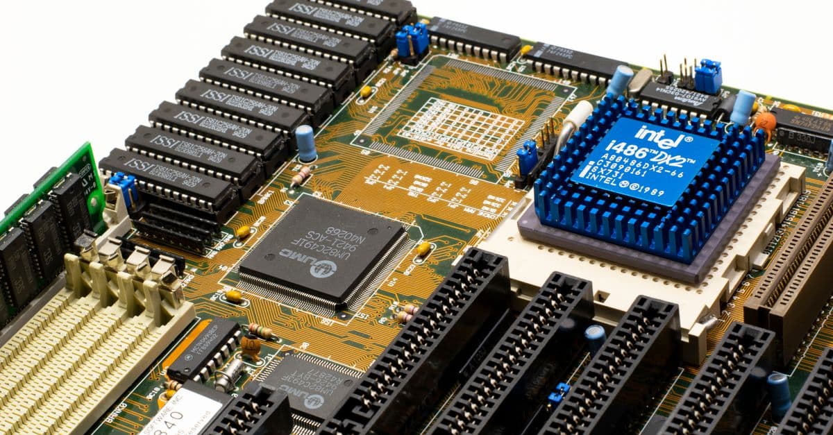
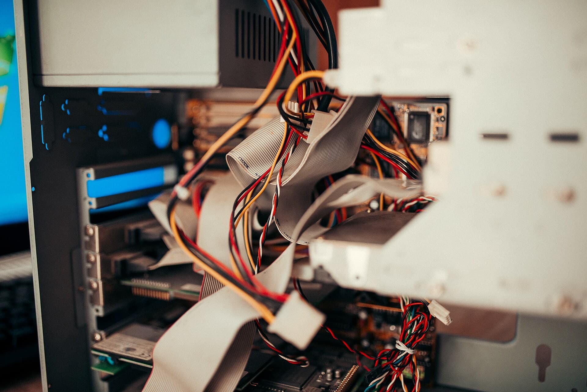
Photo: Nicolas Foster / Pexels
A CPU (central processing unit) is a chip that reads a stream of simple instructions from memory and carries them out, one tiny step at a time, billions of times per second. Everything a computer does, from rendering this page to compressing a photo, reduces to that loop of fetching, decoding, and executing. What separates a 1971 chip from a modern one is not the loop itself but the machinery wrapped around it: pipelines, caches, prediction, and multiple cores. Intel's first microprocessor, the 4004, held 2,300 transistors. Apple says its M4 holds 28 billion. This article follows one instruction through the chip and then widens out to explain why modern CPUs look the way they do.
What a CPU is, and what it is not
A CPU is a programmable digital circuit. "Programmable" is the important word: the chip does not know in advance what job it will do. It reads instructions, which are numbers stored in memory, and each instruction tells it to add two values, move data, compare two numbers, or jump to a different place in the program. Change the numbers in memory and the same silicon does a different job.
The CPU is not the whole computer. The GPU, main memory (RAM), storage, and network hardware all exist partly to feed or serve the CPU. A useful picture is a kitchen. The CPU is the cook, the instructions are the recipe, RAM is the pantry down the hall, and the CPU's own caches and registers are the countertop within arm's reach. Almost everything interesting about CPU design is about keeping the cook busy without sending them to the pantry too often.
Underneath, the chip is built from transistors, tiny electronic switches that are either on or off. Transistors combine into logic gates (AND, OR, NOT), gates into blocks that add or compare numbers, and blocks into a core. That ladder of abstraction is why a chip with tens of billions of parts can still be understood at each level separately. If you want the history of the device that made this possible, see how the transistor changed everything and the invention of the microchip.
The first microprocessor, Intel's 4004, was released in 1971. According to the Computer History Museum, it packed 2,300 transistors into a 4-bit design. Apple's announcement of the M4 in May 2024 says the chip "consists of 28 billion transistors," built on a second-generation 3-nanometer process, with up to four performance cores and six efficiency cores. That is roughly a twelve-million-fold increase in transistor count in 53 years.
One instruction from start to finish
Abstract descriptions of "fetch, decode, execute" hide how mechanical the process is. Here is one concrete instruction, written for RISC-V, the open instruction set described later. The programmer writes:
add x5, x6, x7
This means: take the numbers in registers x6 and x7, add them, and put the result in register x5. A register is a tiny storage slot inside the core. In the RISC-V base instruction set there are 32 integer registers, and the specification notes that register x0 is hardwired to zero, which turns out to be a handy trick for writing constants and discarding results.
To the hardware, the instruction is just a 32-bit number. In RISC-V, every base instruction is 32 bits long. The bits are divided into fields that name the operation and the three registers:
| Field | Bits | Value for this instruction |
|---|---|---|
| funct7 | 31-25 | 0000000 |
| rs2 (second source register) | 24-20 | 00111 (x7) |
| rs1 (first source register) | 19-15 | 00110 (x6) |
| funct3 | 14-12 | 000 |
| rd (destination register) | 11-7 | 00101 (x5) |
| opcode | 6-0 | 0110011 |
Strung together, those fields form the hexadecimal number 0x007302B3. That number is what sits in memory. The CPU never sees the words "add" or "x5." It sees bits, and its circuits are wired so that this particular bit pattern triggers an addition.
Now the cycle:
- Fetch. A register called the program counter holds the memory address of the next instruction. The CPU sends that address to memory, receives the 32-bit pattern, and advances the counter by four bytes so it points at the following instruction.
- Decode. The control logic examines the opcode and function fields and works out what the instruction means. It also reads the two source registers named in the instruction.
- Execute. The two values flow into the arithmetic logic unit (ALU), a circuit that adds, subtracts, and performs bitwise operations. The sum comes out the other side.
- Write back. The result is stored in the destination register, x5. The next instruction can now use it.
Not every instruction touches only registers. A load instruction fetches a value from memory into a register, a store does the reverse, and a branch changes the program counter based on a comparison, which is how if statements and loops work. A program is a long list of these small steps. Nothing mysterious happens at any point; the sophistication comes from doing this very fast and very cleverly.
The loop in the version above would be slow if run literally, because each instruction waits for the previous one to finish all four steps. The next several sections are about the tricks that avoid that wait.
Pipelines: an assembly line for instructions
The first trick is the pipeline. Think of a car factory. Instead of building one car completely before starting the next, the factory splits the work into stations. While one car is being painted, the next is being assembled, and a third is having its engine installed. Each car still takes the same total time, but a finished car rolls out at every station interval instead of at the full build time.
A CPU pipeline does the same with the four steps above. While instruction one is executing, instruction two is being decoded and instruction three is being fetched. In an ideal pipeline, one instruction completes every clock cycle, even though each instruction takes several cycles from start to finish. Real cores use many more than four stages, because splitting the work finer lets the clock run faster.
Pipelines have a weakness: they work well only when the next instruction is predictable. A branch breaks that. When the CPU reaches an if, it does not yet know which instruction comes next, but the pipeline behind it is already filling with whichever guess was made. A wrong guess means the partly processed instructions are thrown away, and the penalty is roughly the depth of the pipeline, since that many cycles of work are lost. This is why branch prediction matters so much, and it is the subject of a later section.
Clock speed, and why gigahertz is not the whole story
The clock is a signal that ticks at a fixed rate and coordinates the chip. A 4 GHz clock ticks four billion times per second. On each tick, the logic in the pipeline advances one step.
Clock speed alone says little about how fast a chip is, because what matters is how much useful work gets done per tick. Engineers call that instructions per cycle (IPC). A rough model of single-thread speed is clock speed multiplied by IPC. As a hypothetical, a chip at 5 GHz averaging 3 instructions per cycle completes 15 billion instructions per second. A chip at 4 GHz averaging 4.5 would complete 18 billion, and would be faster despite the lower clock. Real IPC varies with the program and cannot be read off a spec sheet.
Why not just keep raising the clock? Because of power and heat. A chip's dynamic power draw grows with the square of the supply voltage times the frequency, and higher frequencies generally need higher voltage to switch reliably. Together, that means power rises faster than frequency alone, approaching a cubic relationship in the worst case. Beyond a few gigahertz, a small chip generates more heat per square millimeter than a cooler can remove. Since the mid-2000s, top consumer clock speeds have stayed in the 3 to 6 GHz range, and almost all performance growth since then has come from elsewhere: more cores, wider cores, larger caches, and specialized circuits.
The memory problem, and how caches solve it
A core can perform an addition in a cycle, but fetching data from main memory is vastly slower. Ulrich Drepper's widely cited paper on memory, using Intel figures for a Pentium M, gives approximate access costs in CPU cycles: a register is one cycle or less, the first-level data cache about 3 cycles, the second-level cache about 14, and main memory about 240. Those figures are from the mid-2000s and the exact numbers have shifted since, but the shape has not changed. Memory is hundreds of cycles away.
Drepper traces the cause to the early 1990s, when CPU clock frequencies took off while memory bus speeds and RAM performance did not keep pace. He attributes the gap to cost, not to technical impossibility: RAM as fast as a modern core would be vastly more expensive. This is often called the memory wall.
The answer is the cache, a small, fast memory placed between the core and RAM. Caches work because programs are not random. They tend to reuse data they just touched (temporal locality) and to touch nearby addresses next (spatial locality). Caches exploit the second pattern by moving memory in cache lines, blocks that are 64 bytes in current designs according to Drepper, so fetching one value brings its neighbors along for free.
The usual arrangement has three levels:
| Level | Typical role | Rough size | Shared? |
|---|---|---|---|
| L1 | Fastest, smallest; usually split into instruction and data caches | Tens of kilobytes | One per core |
| L2 | Middle tier | Hundreds of kilobytes to a few megabytes | Usually per core |
| L3 | Last on-chip stop before RAM | Many megabytes | Shared across cores |
One concrete example: Chips and Cheese's analysis of Intel's Golden Cove performance core reports a 1.25 MB L2 cache per core. Sizes differ by design and generation, so treat the table as ranges.
The mathematics of caching explains why it matters so much. Suppose, hypothetically, that 95 percent of memory accesses hit the L1 cache at 3 cycles and 5 percent miss and go to main memory at 240 cycles. The average cost is 0.95 × 3 + 0.05 × 240, about 14.9 cycles. The 5 percent of accesses that miss account for roughly 81 percent of the time. A small drop in the hit rate costs far more than a small improvement in arithmetic speed gains, which is why programmers who care about performance think about how their data is laid out. Walking through a large grid row by row, in the order it is stored, uses each cache line fully. Walking it column by column can pull in a new cache line on nearly every access and run many times slower, though both loops do the same arithmetic.
Doing more per cycle: wide, out-of-order, speculative
Pipelining keeps the stations busy. The next step is to build more than one lane.
Superscalar execution. A modern core has several ALUs and can decode and start multiple instructions in a single cycle. Chips and Cheese's analysis describes Intel's Golden Cove core as six instructions wide at decode, with a 4,000-entry micro-op cache that can deliver eight micro-operations per cycle. If four consecutive instructions do not depend on each other, the hardware can run them side by side.
Out-of-order execution. Programs are written as a sequence, but not every instruction needs the one just before it. If instruction five waits on a slow memory load, instructions six through ten may be able to proceed. An out-of-order core keeps a buffer of upcoming instructions, runs whichever have their inputs ready, and then commits the results in the original program order so the program behaves as written. The size of that buffer, called the reorder buffer, determines how far ahead the core can look. Chips and Cheese reports a 512-entry reorder buffer for Golden Cove, 45 percent larger than its predecessor's. That means hundreds of instructions can be in flight at once.
Branch prediction. Since a wrong guess about a branch flushes the pipeline, cores predict aggressively. The predictor remembers how each branch behaved in the past and uses that history to guess the next outcome. The CPU runs ahead on the guess. If the guess was right, no time was lost. If it was wrong, the work is discarded and the core restarts from the correct path. Chips and Cheese found Golden Cove's predictor performed "very well," while still a hair behind AMD's in their testing. Exact accuracy depends heavily on the program, so be skeptical of any single percentage quoted as universal.
SIMD. Single Instruction, Multiple Data instructions apply one operation to a whole vector of numbers at once, for example adding eight pairs of values with one instruction. Video codecs, image filters, and machine learning code lean on these heavily.
The combination of all four is why a 1990s CPU and a current one can run at similar clock speeds, yet differ in real speed by a large factor.
Speculation has a price: Spectre and Meltdown
Running ahead on a guess is safe only if the discarded work leaves no trace. In January 2018, researchers showed it does. The Spectre paper by Paul Kocher and nine co-authors demonstrated attacks that trick a program into speculatively executing operations it would never perform in correct execution, leaking confidential data through a side channel. The authors found vulnerable speculative execution in processors from Intel, AMD, and ARM. The companion paper, Meltdown, exploited out-of-order execution to read kernel memory on Intel microarchitectures dating back to at least 2010, and stated that "the root cause of Meltdown is the hardware."
The lesson was that performance tricks had quietly become security assumptions. Software workarounds and later hardware changes closed many variants, but the authors of Spectre argued that complete fixes require changes to processor designs and instruction sets, and the episode changed how chip designers weigh speed against isolation.
Cores, threads, and the limits of parallelism
When clock speeds stalled, the industry moved to multiple cores: several complete CPU cores on one chip, each able to run its own stream of instructions. A modern desktop chip may have a handful to a few dozen cores, and server chips have more. Apple's M4 announcement, for instance, cites up to four performance and six efficiency cores.
Cores help only when the work can be divided. Amdahl's Law, a 1967 observation by Gene Amdahl, puts a number on the limit. If a fraction p of a program can run in parallel and the rest must run serially, the best speedup on n cores is 1 divided by ((1 minus p) plus p divided by n). Take a program that is 90 percent parallel. On eight cores the speedup is 1 / (0.1 + 0.1125), about 4.7 times, and no number of cores can push it past 10 times. This is why a 32-core chip does not make everything 32 times faster, and why many everyday tasks (opening a menu, loading a web page) feel unchanged by extra cores.
Simultaneous multithreading (SMT), which Intel markets as Hyper-Threading, lets one core present itself as two. It duplicates some bookkeeping but shares the execution units, so when one thread stalls waiting for memory, the other can use the idle hardware. The gain is real but well short of doubling, because the two threads compete for the same resources. Some designs skip it entirely in favor of wider cores.
Many mobile and laptop chips now pair performance cores with efficiency cores, a design often called big.LITTLE. Apple's M1, introduced in November 2020, has four high-performance and four high-efficiency cores, and Apple stated the efficiency cores "deliver outstanding performance at a tenth of the power." The operating system steers demanding work to the big cores and background chores to the small ones, which saves battery.
Instruction set architectures: x86, ARM, and RISC-V
The instruction set architecture (ISA) is the contract between software and hardware: the vocabulary of instructions a CPU understands. Two chips with different internal designs can implement the same ISA and run the same programs. Programs compiled for one ISA do not run natively on another.
| Feature | x86-64 | ARM | RISC-V |
|---|---|---|---|
| Style | Complex (CISC) | Reduced (RISC) | Reduced (RISC) |
| Roots | Intel, from the late 1970s | Arm, a UK company founded around a 12-person team in a Cambridge barn | Started May 2010 at UC Berkeley's Par Lab |
| Licensing | Proprietary to Intel and AMD | Licensed from Arm | Open; the base design was released under a BSD license |
| Instruction length | Variable, 1 to 15 bytes | Mostly fixed 32-bit in 64-bit mode | Fixed 32-bit base, optional 16-bit compressed form |
| Typical homes | PCs, many servers | Phones, tablets, Apple laptops, cloud chips | Embedded devices, research, custom accelerators |
The RISC-V details come from its own history page. The instruction set was started in May 2010 at Berkeley's Parallel Computing Laboratory by Krste Asanovic and students Yunsup Lee and Andrew Waterman, under David Patterson's lab. The RISC-V Foundation was founded in 2015 with 36 founding members and became RISC-V International, incorporated in Switzerland, in March 2020.
The practical difference between "complex" and "reduced" is about decoding. In x86, instructions vary in length, so the decoder must work out where each one ends before it can start the next, which adds complexity. In a fixed-length ISA, the hardware can chop the instruction stream into slices without examining the contents, which makes it easier to decode several instructions per cycle. Modern x86 chips work around this by translating instructions into simpler internal micro-operations, which is why the "CISC versus RISC" distinction matters less inside the chip than it did in the 1980s. It still affects power and design effort.
The business difference is equally important. x86 is controlled by two companies. ARM chips come from a licensing model in which Arm sells designs and architecture rights and others build the chips; Arm's Flexible Access program, for example, gives low-cost access to its designs with license fees due only at tape-out, the point where a design is sent to be manufactured. RISC-V is open, which lets any company build a chip without a license fee for the base design.
The Apple Silicon case study
In November 2020, Apple announced the M1, a laptop CPU that it claimed delivered "up to 3.5x faster CPU performance" than previous-generation Macs and "the world's best CPU performance per watt." Those are Apple's own claims from its own testing, and the numbers should be read that way. What is not disputed is the design approach, which illustrates the ideas in this article.
First, Apple's M1 was a system on a chip. The CPU cores, GPU, neural engine, and memory controllers sat on one piece of silicon built on a 5-nanometer process with 16 billion transistors, per Apple's announcement. Second, it used a unified memory architecture: Apple described a single pool of high-bandwidth, low-latency memory that all the components can access "without copying it between multiple pools of memory." Avoiding copies matters because moving data is often more expensive, in time and energy, than computing on it. Third, it adopted the big/little core arrangement described above. Fourth, Apple designed the chip, the operating system, and much of the software together, so it could tune each for the others.
M1 started a shift in the laptop market. Qualcomm, Microsoft, and others have since pushed ARM chips into Windows laptops. The result is less a replacement of one ISA by another than a broader point: with the same transistor budget, a chip designed around power efficiency and tight integration can compete with designs built around raw clock speed.
Moore's Law and what replaced it
Gordon Moore's 1965 paper predicted that the number of components on a chip would double every year for the next 10 years. In 1975, he revised the period to every two years, according to Intel's summary of the history. The doubling held, with variations, for decades, and the gap between the 4004's 2,300 transistors and the M4's 28 billion is the visible result.
What kept it going was shrinking the transistor. But the numbers in process names no longer measure anything physical. An IEEE Spectrum analysis explains that node names have been disconnected from real feature sizes since the mid-1990s: the 130-nanometer node had gates about 70 nanometers long, and Intel's 22-nanometer chips in 2011 had a gate length of 26 nm, a metal half-pitch of 40 nm, and fins 8 nm wide. The article quotes the statement that most critical features of a "7-nm" transistor are considerably larger than 7 nm. Today's "3 nm" and "2 nm" are generation labels. Industry groups have proposed replacing them with density-based measures, such as a notation based on contacted gate pitch and metal pitch (the article gives 48 nm and 36 nm for a coming 5-nm chip).
Progress has continued through new transistor shapes rather than smaller labels. TSMC states that its 2-nanometer-class N2 technology entered volume production in the fourth quarter of 2025, using a first-generation nanosheet transistor design. To learn how these chips are physically made, see how semiconductors are made, how fabs work, and the EUV lithography explainer.
Three other responses to the slowing of simple scaling are visible across the industry:
- Chiplets. Instead of one huge die, a processor is assembled from several smaller ones in a single package, which improves yield and lets companies mix manufacturing processes. See why chiplets are changing processor design.
- Specialization. Dedicated blocks for video, AI, and cryptography do those jobs with far less energy than a general-purpose core. The GPU explainer covers the most important example.
- Better software and memory design. Since moving data is costly, improvements in caches, memory bandwidth, and software layout now deliver gains that raw transistor counts used to.
CPU versus GPU
A GPU is also a processor, optimized for a different job. A CPU has a modest number of complex cores built to run varied, branch-heavy code with low latency. A GPU has many simpler cores built to run the same operation across large amounts of data at once. Graphics, scientific simulation, and machine learning fit the second pattern. Operating systems, databases, and web browsers fit the first. They are complementary, and a modern computer uses both. Under heavy load, both can overheat and slow themselves down; why thermal throttling slows devices explains how.
What this means
A CPU is less a single clever invention than a stack of workarounds, each answering a limit left by the one before. The basic loop was too slow, so engineers added pipelines. Pipelines stalled on branches, so they added prediction. Memory lagged behind, so they added caches. Clock speeds hit a heat ceiling, so they added cores. Each fix created a new problem, from security holes like Spectre to the limits of parallel speedup.
That pattern explains where the field is going. With simple shrinking no longer guaranteed, gains now come from smarter organization: moving less data, doing more per cycle, using specialized hardware, and designing chips and software together. The 1971 chip and the current one run the same loop. The difference is everything built to keep that loop from waiting.
Frequently asked questions
Q: What does a CPU actually do? A: It repeatedly fetches an instruction from memory, decodes what it means, executes it using circuits such as the arithmetic logic unit, and writes the result to a register or memory. Programs are long sequences of such simple instructions, including arithmetic, data movement, comparisons, and jumps.
Q: Is a higher clock speed always better? A: No. Performance depends on clock speed multiplied by how many instructions complete per cycle, and on how well the workload uses cache, memory, and multiple cores. A lower-clocked chip with higher instructions per cycle can outperform a higher-clocked one.
Q: Why don't CPUs just keep getting faster in gigahertz? A: Power and heat. Dynamic power rises with voltage squared times frequency, and higher frequencies usually need higher voltage, so power climbs faster than speed. Since the mid-2000s, mainstream clocks have stayed in the 3 to 6 GHz range, and designers have added cores, cache, and specialized units instead.
Q: What is cache, and why does a CPU need it? A: Cache is small, fast memory on the chip that holds recently used data and its neighbors. Main memory is hundreds of cycles away; Drepper's Intel-based figures put it at about 240 cycles versus about 3 for the first-level cache. Without caches, cores would spend most of their time waiting.
Q: What does the "nanometer" in 3 nm or 2 nm mean? A: Today it is a generation label, not a measurement. IEEE Spectrum reports that node names have been disconnected from real feature sizes since the mid-1990s, and that most critical features of a "7-nm" transistor are considerably larger than 7 nm.
Q: What is the difference between x86, ARM, and RISC-V? A: They are different instruction sets. x86 is proprietary to Intel and AMD and uses variable-length instructions. ARM is licensed by Arm and common in phones and Apple chips. RISC-V began at UC Berkeley in 2010 and is open, so anyone can build a chip without paying a license fee for the base design.
Q: What were Spectre and Meltdown? A: Two hardware security flaws disclosed in January 2018. Both exploited speculative or out-of-order execution to leak data through side channels. Spectre affected Intel, AMD, and ARM processors; Meltdown affected Intel microarchitectures going back to at least 2010, according to the researchers.
Sources
- Computer History Museum. Microprocessor integrates CPU function onto a single chip (Intel 4004, 1971, 2,300 transistors).
- Apple (2024). Apple introduces M4 chip.
- Apple (2020). Apple unleashes M1.
- Intel. Moore's Law.
- Drepper, U. (2007). What every programmer should know about memory, part 2: CPU caches, LWN.net.
- Chips and Cheese. Popping the hood on Golden Cove.
- Kocher, P., et al. (2018). Spectre Attacks: Exploiting Speculative Execution.
- Lipp, M., et al. (2018). Meltdown.
- IEEE Spectrum. A Better Way to Measure Progress in Semiconductors.
- TSMC. 2nm Technology.
- RISC-V International. History of RISC-V and the RISC-V unprivileged ISA specification.
- Arm. Company overview.
- Hennessy, J., and Patterson, D. (2019). Computer Architecture: A Quantitative Approach, 6th ed.
- Amdahl, G. (1967). Validity of the single processor approach to achieving large scale computing capabilities. AFIPS Spring Joint Computer Conference.
Related reading
Follow new articles
Add SciHub101 to your feed reader to see new science and technology stories.
About the Author
SciHub101 is an independent science and technology publication founded and edited by Buğra Sözeri, a software engineer and app developer based in Türkiye. AI tools assist with drafting and research. Source documentation in the existing archive is uneven, and articles are being reviewed and corrected. The Editorial Team byline identifies editorial responsibility; it does not certify specialist or independent human review. Where we compare products, anything built by our own team is labelled as such — see the editorial guidelines and About page for how corrections and disclosures work.
Related Articles

Blockchain Explained — Beyond Bitcoin
How blockchains actually work, consensus mechanisms compared, smart contracts, what blockchain is good for, and what it isn't — balanced view for 2026.
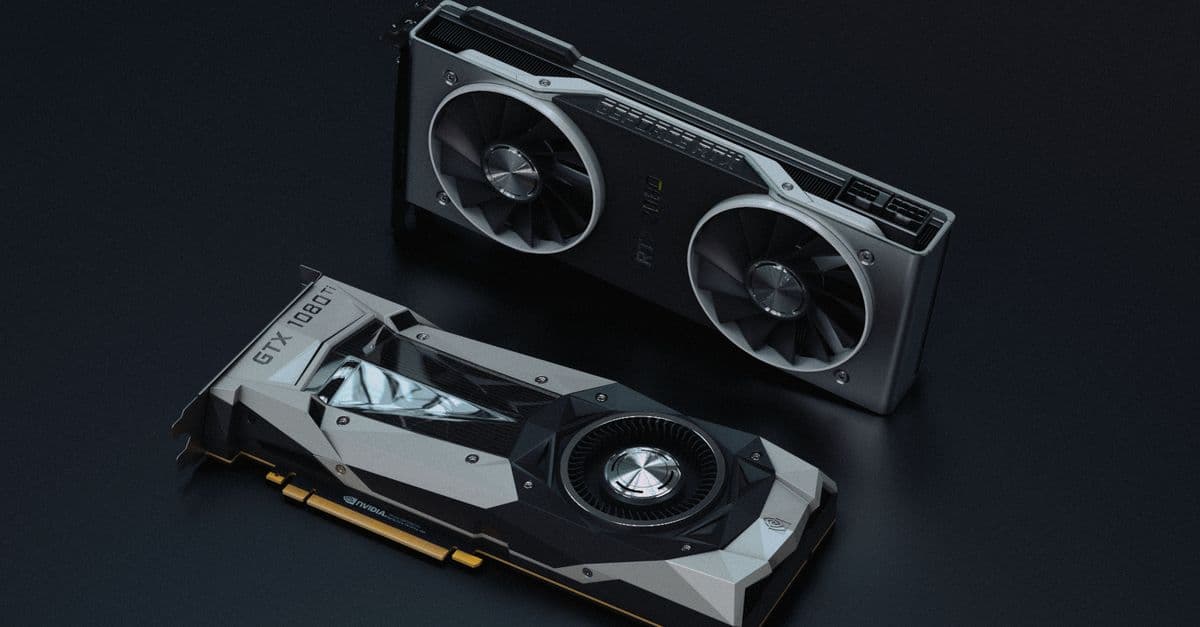
How GPUs Work — Why AI Needs Them
How GPUs run thousands of threads at once, what tensor cores and HBM memory do, and why neural network training maps so well onto GPU architecture.
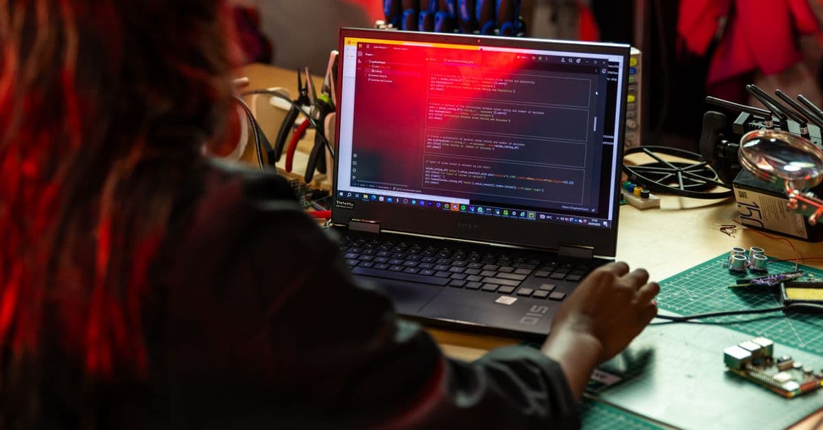
How to Choose the Right Laptop in 2026: A Practical Buyer's Guide
A laptop purchase is a $1,000-$3,000 decision that you will live with for 4-5 years. The specifications that matter depend entirely on your use case: a student writing essays needs different hardware than a software developer compiling code or a video editor rendering footage. CPU, GPU, RAM, and storage determine performance; display quality and battery life determine daily usability. The trap is specification obsession—comparing gigahertz and cores without understanding actual workload demands. This guide breaks down what each component means, the realistic use-case tiers (student, creator, developer, gamer), the hardware tradeoffs, and the mistakes that lead to wrong purchases. A $600 laptop perfectly suited to your needs serves you better than a $2,500 laptop that is over-specified for your work.
How AI Designs Chips: Hardware-Aware Neural Architecture Search
AI now helps design the chips that run AI. Reinforcement-learning floorplanning, neural architecture search, and co-design are changing semiconductor R&D, and parts of the evidence are disputed.
Complete Technology Guide 2026 — How Modern Tech Works
The complete guide to technology in 2026: how the internet, semiconductors, and quantum computing work, AI hardware, cybersecurity, and what's coming next.

How Microphones Work — From Sound Waves to Electrical Signals
A microphone is a transducer that converts pressure waves in air into electrical signals, and there are at least six fundamentally different ways to accomplish that conversion, each with trade-offs in sensitivity, ruggedness, and frequency response.