How the Transistor Changed Everything
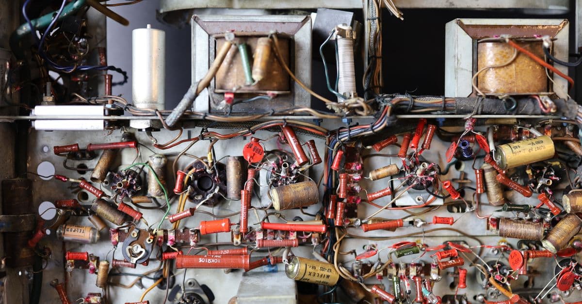
Photo: Lech Pierchała / Pexels
Every smartphone, laptop, car engine controller, pacemaker, satellite and data centre runs on the same basic component: a tiny electrical switch with no moving parts. Every digital calculation ever performed has been a sequence of those switches turning on and off. Social media, online banking, weather forecasts and chatbots all reduce, physically, to that one device.
The transistor is arguably the most important invention of the 20th century, and by count one of the most manufactured objects humans have ever made. A single modern AI processor holds more of them than there are people on Earth many times over. Yet most people who use billions of transistors every day could not explain what one does. This article explains it: the problem it solved, the December 1947 experiment at Bell Labs, how a transistor actually switches, how the MOSFET and the integrated circuit turned it into a mass-produced commodity, and what happens now that its features are only a few dozen atoms across.
Key Takeaways
- Bell Labs physicists John Bardeen and Walter Brattain demonstrated the first transistor, a germanium point-contact device, in December 1947; William Shockley led their group
- The three shared the 1956 Nobel Prize in Physics "for their researches on semiconductors and their discovery of the transistor effect"
- The MOSFET, built at Bell Labs by Mohamed Atalla and Dawon Kahng in 1959, became the transistor type used in almost every modern chip
- The integrated circuit (1958–59) and Gordon Moore's 1965 forecast turned transistors into a product that improved on a predictable schedule
- Transistor counts went from 2,300 on Intel's 4004 (1971) to 208 billion on NVIDIA's Blackwell GPU (announced 2024)
- Shrinking now relies on 3D transistor shapes and chip stacking rather than simple flat scaling
The Problem with Vacuum Tubes
To understand why the transistor mattered, start with what it replaced. The vacuum tube, developed in the first decade of the 1900s, was the electronic switch and amplifier of its era. A heated filament released electrons into a vacuum, and a voltage on a wire mesh, the grid, controlled how many reached a collecting plate. A small signal on the grid could control a large current, which is amplification. Driven hard, the same tube acted as an on/off switch. Tubes powered radio, television, radar, long-distance telephony and the first electronic computers.
They also had serious limits. Each tube was roughly the size of a light bulb, used watts of power just to keep its filament hot, generated heat that had to be removed, and eventually burned out. The Computer History Museum's timeline describes ENIAC, unveiled in 1946, as using about 18,000 vacuum tubes and weighing 30 tons. At that scale, failures were a routine operational problem, and a large share of an engineer's time went to finding and replacing dead tubes.
The deeper problem was that tubes could not shrink much. They needed an evacuated glass or metal envelope and a heated cathode. There was no plausible path to a tube the size of a grain of sand, let alone a billion of them on a fingernail.
Bell Telephone Laboratories in Murray Hill, New Jersey, had a strong commercial reason to care. The American telephone network used tubes to amplify signals over long distances and electromechanical relays to switch calls, and both were bulky, power-hungry and failure-prone. According to the Computer History Museum, Shockley started a solid-state physics group at Bell Labs in 1945 specifically to look for semiconductor replacements for tubes and relays.
Semiconductors: The Material That Made It Possible
Semiconductors such as germanium and silicon conduct electricity better than insulators like glass but much worse than metals like copper. Their key property is that their conductivity can be controlled, by temperature, light, electric fields and, above all, by adding tiny amounts of impurity atoms, a process called doping.
- n-type doping adds atoms such as phosphorus or arsenic, which have one more outer electron than silicon. The extra electrons are free to carry current.
- p-type doping adds atoms such as boron, which have one fewer. The resulting gaps, called holes, move through the crystal like positive charges.
Where n-type and p-type regions meet, a junction forms with a thin "depletion" zone that resists current in one direction. Junctions and the electric fields around them are the raw material of every transistor. The quantum mechanics behind this, band theory, was worked out in the 1930s; without it, the Bell Labs team would have had no theory to guide their experiments. For a refresher on charge and current themselves, see How Electricity Works.
December 1947: The Point-Contact Transistor
Shockley's first idea was a field-effect amplifier: use an electric field to change the conductivity of a thin semiconductor layer. It did not work. Bardeen proposed that electrons trapped at the semiconductor's surface, called surface states, were screening the field. Investigating those surface states led Bardeen and Brattain to a different device.
According to the Computer History Museum, on December 16, 1947 they pressed two closely spaced gold contacts, held by a plastic wedge, onto a slab of high-purity germanium. A small signal on one contact changed the current through the other, amplifying it by up to 100 times. On December 23 they demonstrated it to Bell Labs management, and Shockley called it "a magnificent Christmas present". Bell Labs announced the device publicly at a press conference in New York on June 30, 1948. The name "transistor", a blend of "transfer" and "resistor", came from the Bell Labs engineer John Pierce.
Shockley, reportedly frustrated at not being part of the key experiment, quickly worked out the theory of a sturdier design, the junction transistor, in which current is controlled through layered n-p-n or p-n-p regions inside the crystal. Junction transistors were far easier to manufacture reliably than the delicate point-contact device and dominated the 1950s. The three men shared the 1956 Nobel Prize in Physics. Shockley later founded Shockley Semiconductor Laboratory in Mountain View, California; eight of his employees left in 1957 to form Fairchild Semiconductor, an event that helped create Silicon Valley. Our inventions article The Invention of the Transistor goes deeper into the people and the patent history.
How a Transistor Actually Works
There are two big families of transistor, and it helps to keep them separate.
Bipolar junction transistors (BJTs) have three terminals called the emitter, base and collector. A small current into the base controls a much larger current from collector to emitter. BJTs were the workhorses of early transistor radios and computers and are still used in some analog and high-power circuits.
Field-effect transistors (FETs), and specifically MOSFETs (metal-oxide-semiconductor field-effect transistors), have terminals called the source, drain and gate. Current flows from source to drain through a channel of semiconductor. The gate sits above the channel, separated from it by a very thin insulating layer, originally silicon dioxide. A voltage on the gate creates an electric field that attracts or repels charge carriers in the channel, turning it conductive or not. Gate voltage above a threshold: the switch is on. Below it: off.
The crucial advantage of the MOSFET is that the gate draws almost no steady current, because it is insulated. That means a MOSFET switch uses very little power except at the moment it switches, which is what makes billions of them on one chip practical. The most common digital design, CMOS (complementary MOS), pairs an n-channel and a p-channel MOSFET so that in either steady state one of them is off, further cutting wasted power.
Combine a few transistors and you get logic gates. Two MOSFETs in series form part of a NAND gate, whose output is 0 only if both inputs are 1. Any logical function, and therefore any computation, can be built from NAND gates alone. That connection between switches and Boolean logic was first made explicit by Claude Shannon in his 1937 MIT thesis on relay circuits, described in Claude Shannon: The Bell Labs Tinkerer Who Invented Information.
| Feature | Vacuum tube (triode) | Bipolar junction transistor | MOSFET |
|---|---|---|---|
| Control signal | Voltage on grid | Current into base | Voltage on insulated gate |
| Needs heated filament | Yes | No | No |
| Steady-state control current | Very small | Significant | Nearly zero |
| Typical use today | Niche audio, high-power RF | Analog, power, RF circuits | Virtually all digital chips |
| Can be scaled to nanometres | No | Limited | Yes |
The MOSFET: The Transistor That Took Over
The Computer History Museum credits Mohamed (John) Atalla and Dawon Kahng at Bell Labs with the first successful insulated-gate field-effect transistor in 1959, building on Atalla's work on growing stable silicon dioxide layers on silicon. Bell Labs initially showed limited interest, because early MOSFETs were slower than bipolar devices. Other labs pushed ahead: an RCA team built an experimental integrated device with 16 MOS transistors in 1962, and MOS devices reached the commercial market in 1964, according to the same source.
The decisive advantage was manufacturing. MOSFETs are flat, can be made with a small number of process steps on the surface of a silicon wafer, and shrink well: when you scale all dimensions down, they get faster and use less power per switch. In 1974 IBM engineer Robert Dennard and colleagues described the rules for this, known as Dennard scaling. For about three decades it meant that every new generation of chips was smaller, faster and more power-efficient all at once.
The Integrated Circuit and Moore's Law
Early transistors were discrete parts, soldered one by one onto circuit boards. As circuits grew to thousands of components, the wiring itself became the bottleneck. In 1958 Jack Kilby at Texas Instruments built a working circuit on a single piece of germanium. In 1959 Robert Noyce at Fairchild Semiconductor described a silicon version using the planar process developed by his colleague Jean Hoerni, with metal interconnections deposited directly onto an insulating oxide layer. Noyce's approach was the one that scaled. Microchip Invention: Kilby, Noyce, and the Integrated Circuit tells that story in full.
The integrated circuit changed the economics of electronics. Transistors and their connections are made together by photolithography, printing patterns through masks with light, so a wafer full of chips costs roughly the same to process regardless of how many transistors each chip contains. Shrinking the features meant more transistors per wafer for nearly the same cost.
In April 1965 Gordon Moore, then Fairchild's director of research and development, published "Cramming more components onto integrated circuits" in Electronics magazine. According to the Computer History Museum, he plotted components per chip from 1959 to 1964, projected a doubling every year, and estimated about 65,000 components on a chip by 1975. In 1975, by then at Intel, which he had co-founded with Noyce in 1968, he revised the pace to a doubling every two years. The forecast, nicknamed Moore's Law, became a shared target for chipmakers and equipment suppliers.
Transistor Counts Over Time
The table uses figures published by the chipmaker or a recognised record body. Counts are for the whole chip, and the AI accelerator figures include very large dies or multi-die packages, so they are not directly comparable with a phone processor.
| Chip | Year | Transistors | Source |
|---|---|---|---|
| Intel 4004 | 1971 (on sale Nov 15) | 2,300 | Guinness World Records |
| Apple M1 | 2020 | 16 billion | Apple Newsroom, Nov 10, 2020 |
| NVIDIA H100 (Hopper) | 2022 (announced Mar 22) | 80 billion | NVIDIA Newsroom |
| NVIDIA Blackwell GPU | 2024 (announced Mar 18) | 208 billion | NVIDIA Newsroom |
From 2,300 to 208 billion is a factor of about 90 million in 53 years, which works out to a doubling roughly every two years, very close to Moore's revised forecast. No other manufactured product has improved at a comparable rate for so long. Apple described the M1 as built on a 5-nanometre process, and NVIDIA built Hopper on TSMC's 4N process and Blackwell on a custom 4NP process. Those processes and the people who use them have reshaped everything from the personal computer to the smartphone.
How Billions of Transistors Are Made
A modern chip starts as a polished wafer of nearly pure single-crystal silicon. The transistors are built on its surface layer by layer, through a loop of steps repeated many times:
- Deposition. A thin film of material, such as an insulator, a metal or a doped semiconductor, is grown or deposited across the whole wafer.
- Coating. The wafer is covered with photoresist, a light-sensitive polymer.
- Lithography. Light shines through a patterned mask, called a reticle, and a system of lenses projects a reduced image of the pattern onto the resist. At the leading edge, this uses extreme ultraviolet light with a wavelength of 13.5 nanometres, which has to be handled with mirrors in a vacuum because ordinary lenses and air absorb it.
- Etching. Chemicals or plasmas remove material wherever the resist pattern leaves it exposed.
- Doping. Ion implantation fires dopant atoms into selected regions to set their electrical type.
- Cleaning and inspection. Residue is stripped and the wafer is checked for defects before the next layer.
A leading-edge chip goes through this loop for hundreds of individual process steps. The transistors themselves are formed at the bottom, and above them a dozen or more layers of copper wiring connect them into circuits. A single speck of dust can ruin a chip, which is why fabrication plants filter their air far more strictly than a hospital operating theatre.
The defining economic fact is that all the transistors on a wafer are made at once. Adding more transistors to a chip design costs area, not extra assembly labour. That is why counts could climb from thousands to billions while the price of an individual transistor fell to a tiny fraction of a cent. It is also why the industry has consolidated: a single leading-edge factory now costs many billions of dollars, and only a handful of companies worldwide can build chips at the most advanced processes.
What the Transistor Made Possible
Computers are the obvious answer, but the transistor's impact started elsewhere. The first commercial products were hearing aids in the early 1950s, followed by the pocket transistor radio, which made portable broadcast listening ordinary for the first time and helped spread popular music worldwide. The history of broadcast technology up to that point is told in The Radio: Marconi, Tesla, and the Invention That Wired the Air.
Spaceflight depended on solid-state electronics because every gram and every watt mattered. Telephone exchanges moved from relays to transistor switching. Digital watches, calculators, video game consoles, digital cameras, GPS receivers, mobile phones and modern medical imaging all followed. Today a car contains many microcontrollers, and power transistors made from materials such as silicon carbide manage the batteries and motors in electric vehicles.
The same scaling now drives artificial intelligence. Training a large neural network involves enormous numbers of multiply-and-add operations, each executed by transistor logic, which is why AI progress has tracked chip progress so closely. It is also why the electricity demands of computing have become a policy issue, discussed in How AI Data Centers Use Electricity.
Common Misconceptions
"A 3-nanometre chip has transistors 3 nanometres wide." Not any more. Process names such as "5 nm" or "3 nm" are generation labels. Since the late 1990s they have drifted away from any single physical dimension, and actual gate pitches and metal spacings are considerably larger than the name suggests.
"Shockley invented the transistor." Bardeen and Brattain built and demonstrated the first device; Shockley led the group, devised the junction transistor and shared the Nobel Prize. Credit was a source of lasting tension among the three.
"Transistors are only for computing." Analog transistors amplify audio, radio and sensor signals, and power transistors switch large currents in chargers, motor drives and the electricity grid.
"Moore's Law means computers double in speed every two years." The forecast was about the number of components per chip at minimum cost. Clock speeds largely stopped climbing in the mid-2000s, when Dennard scaling broke down and chips hit power and heat limits. Performance gains since then have come mostly from more cores and specialised circuits.
Where Transistors Go Next
Silicon atoms in a crystal are spaced about 0.54 nanometres apart (the lattice constant), so the most critical features of today's transistors are only a few dozen atoms across. At these sizes, electrons can tunnel through insulating barriers they would classically be unable to cross, which causes current to leak when a transistor should be off. The physics of that effect is explained in Quantum Tunneling: How Particles Pass Through Walls.
The industry's answer has been to change the transistor's shape. FinFETs, which entered high-volume production in the early 2010s, stand the channel up as a thin vertical fin with the gate wrapped around three sides, giving better control. Gate-all-around designs, also called nanosheet or ribbon transistors, surround the channel on all sides and are now entering production at the leading chipmakers. Beyond that, researchers are working on stacking n-type and p-type transistors on top of each other, delivering power from the back of the wafer, and packaging several smaller chips, called chiplets, together. NVIDIA's 208-billion-transistor Blackwell figure is itself a two-die package.
New channel materials are also under study, including two-dimensional semiconductors only a few atoms thick, carbon nanotubes and compound semiconductors such as gallium nitride, which is already common in compact phone chargers. Quantum computing is a different paradigm rather than a replacement; it uses qubits for particular kinds of problems while still relying on classical transistor electronics to control them. See How Do Quantum Computers Actually Work? for that comparison.
Whatever replaces today's silicon transistor will very likely still be a device that uses an electric field to switch current on and off. The geometry and materials will keep changing; the idea Bardeen, Brattain and Shockley proved in 1947 probably will not.
FAQ
Q: What exactly does a transistor do? A: It is a three-terminal semiconductor device that switches or amplifies electrical signals. In a MOSFET, the voltage on the gate controls whether current flows between source and drain. Billions of these switches represent and process binary data in a computer.
Q: Who invented the transistor? A: John Bardeen and Walter Brattain built and demonstrated the first point-contact transistor at Bell Labs in December 1947, in a group led by William Shockley, who soon designed the junction transistor. All three shared the 1956 Nobel Prize in Physics.
Q: What is a MOSFET and why does it matter? A: A MOSFET is a field-effect transistor whose gate is insulated from the channel by a thin oxide layer. First demonstrated by Atalla and Kahng at Bell Labs in 1959, it uses very little power when idle and shrinks well, which is why it is the transistor type in nearly all modern digital chips.
Q: What is Moore's Law? A: It is Gordon Moore's 1965 forecast that the number of components on an integrated circuit would double every year, revised in 1975 to every two years. It is an industry trend rather than a physical law, and the pace has slowed as transistors approach atomic dimensions.
Q: How many transistors are in a modern chip? A: It depends on the chip. Apple's M1 laptop processor of 2020 has 16 billion; NVIDIA's H100 AI accelerator of 2022 has 80 billion; NVIDIA's Blackwell GPU, announced in 2024, has 208 billion across two dies.
Q: Are we running out of room to shrink transistors? A: Simple flat scaling has largely ended, because leakage from quantum tunnelling and heat limit how small features can get. The industry continues to add transistors through 3D shapes such as FinFETs and gate-all-around designs, stacking and multi-chip packaging, but each step is harder and more expensive.
Sources
- Computer History Museum, 1947: Invention of the Point-Contact Transistor
- Computer History Museum, 1960: Metal Oxide Semiconductor (MOS) Transistor Demonstrated
- Computer History Museum, 1965: "Moore's Law" Predicts the Future of Integrated Circuits
- Computer History Museum, Timeline of Computer History (ENIAC)
- Guinness World Records, First microprocessor
- Apple Newsroom, Apple unleashes M1 (November 10, 2020)
- NVIDIA Newsroom, NVIDIA Announces Hopper Architecture (March 22, 2022)
- NVIDIA Newsroom, NVIDIA Blackwell Platform Arrives to Power a New Era of Computing (March 18, 2024)
- The Nobel Prize in Physics 1956, nobelprize.org (citation wording)
Read next:
Follow new articles
Add SciHub101 to your feed reader to see new science and technology stories.
About the Author
SciHub101 is an independent science and technology publication founded and edited by Buğra Sözeri, a software engineer and app developer based in Türkiye. AI tools assist with drafting and research. Source documentation in the existing archive is uneven, and articles are being reviewed and corrected. The Editorial Team byline identifies editorial responsibility; it does not certify specialist or independent human review. Where we compare products, anything built by our own team is labelled as such — see the editorial guidelines and About page for how corrections and disclosures work.
Related Articles

AI Software Testing: How Machine Learning Finds Bugs Early
Machine learning now helps pick which tests to run, steer fuzzers toward crashes, draft unit tests, and flag anomalies in production. Here is what published results show, and where the tools still fail.

Computer Vision Object Detection Explained: From YOLO to Vision Transformers
Object detection went from slow two-stage pipelines to real-time single-pass networks and transformer detectors. Here is how each generation works and what the benchmark numbers mean.
Semiconductor Chips: How They Work
A modern processor packs tens of billions of transistors onto a sliver of silicon. Here is how doped silicon becomes switches, switches become logic, and logic becomes a computer.

History of Aviation: From the Wright Brothers to Today
On December 17, 1903, Orville Wright flew 120 feet in 12 seconds. In 2024, airlines carried about 4.7 billion passengers. Here is how the engineering got from one to the other.
History of Electricity: Faraday, Tesla, Edison, and the Force That Powers the World
Electricity was a scientific curiosity in 1800. Within 100 years it was lighting cities and running factories.

How Solar Panels Convert Light to Electricity
A photon from the sun hits silicon, kicks out an electron, and creates electricity. This simple fact is reshaping civilization.