Semiconductor Chips: How They Work
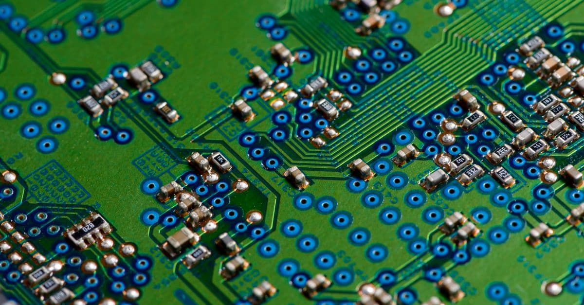
Photo: Júlio Riccó / Pexels
Apple's M3 processor, announced on October 30, 2023, contains 25 billion transistors. Each one is an electrically controlled switch, and each switch is built from silicon that has been deliberately contaminated with a few atoms of other elements. The same trick, repeated billions of times and wired together in layers, is what lets a sliver of material run a phone, a laptop, or a data center. This article explains how that works, starting from the atoms and ending at the arithmetic, memory, and limits of the modern chip.
Key takeaways
- A semiconductor is a material whose ability to conduct electricity can be tuned. Silicon is the standard choice because it is abundant, forms a stable oxide, and can be purified to extreme levels.
- Doping silicon with a tiny amount of phosphorus or boron creates n-type or p-type material. A boundary between the two is a diode, and a gate placed over a channel makes a MOSFET, the switch used in nearly all digital chips.
- Pairing n-type and p-type transistors gives CMOS logic, which draws little power when idle and forms gates, adders, and processors.
- Memory uses the same transistors in different arrangements: one transistor and a capacitor for DRAM, six transistors for SRAM, and trapped charge for flash.
- Node names such as "3 nm" are marketing labels. Real limits now come from heat, leakage current, and manufacturing cost.
Why silicon, and what a semiconductor actually is
Materials sort roughly into three groups by how easily they carry current. Metals like copper have electrons that move freely. Insulators like glass hold their electrons tightly. Semiconductors sit between the two, and their conductivity can be shifted by temperature, light, or added impurities.
The physics behind that middle position is the band gap, the energy an electron needs to jump from being bound to an atom to being free to carry current. Silicon's band gap is 1.12 electron volts. At room temperature only a trickle of electrons gets that energy: the intrinsic carrier concentration of silicon is about 1.08 × 10¹⁰ per cubic centimeter, in a crystal containing about 5 × 10²² atoms per cubic centimeter. Put differently, roughly one atom in five trillion contributes a free electron. Pure silicon is a poor conductor, which is precisely what makes it controllable.
Silicon is also the second most abundant element in Earth's crust by mass, after oxygen, and it forms a tough, stable native oxide (silicon dioxide, the main ingredient of glass and sand). That oxide matters as much as the silicon. It is an excellent insulator, it grows cleanly on the crystal surface, and for decades it served as the gate dielectric in transistors.
Doping: contamination on purpose
Doping adds a controlled trace of another element to the silicon crystal. Light doping runs to about one dopant atom per 100 million silicon atoms, and heavy doping to about one per 10,000. Two types do almost all the work.
- N-type silicon is doped with a Group V element such as phosphorus. Each phosphorus atom brings one electron more than the silicon lattice needs, and that extra electron is free to move. The charge carriers are negative.
- P-type silicon is doped with a Group III element such as boron, which has one electron too few. The missing electron is called a hole, and a hole acts like a mobile positive charge as neighboring electrons hop into it.
A useful analogy is a parking garage. N-type silicon is a garage with a few extra cars wandering the aisles. P-type silicon is a nearly full garage with a few empty spaces, where the movement you see is cars shuffling into the gaps and the gaps appearing to move the other way. Either way, the doping level, not the temperature, sets how much current is available.
The p-n junction
Join p-type and n-type silicon and electrons from the n side diffuse across and fill holes on the p side. This leaves a thin depleted region with almost no free carriers and a built-in electric field. Current can flow easily in one direction (when an outside voltage pushes carriers toward the junction) and barely at all in the other. That one-way behavior is a diode, and it is the building block of rectifiers, LEDs, and solar cells. A transistor is, in essence, a junction structure with a third terminal that can open or close it.
The transistor and the MOSFET
In 1947, John Bardeen and Walter Brattain produced a semiconductor amplifier at Bell Labs, which William Shockley then developed further. The three shared the 1956 Nobel Prize in Physics "for their researches on semiconductors and their discovery of the transistor effect." The full story of that device and its successors is told in the companion piece on how the transistor changed everything (linked under Read next).
That first device was a bipolar transistor, which needs a steady trickle of current to stay on. The design that took over computing is the MOSFET, short for metal-oxide-semiconductor field-effect transistor. Mohamed Atalla and Dawon Kahng at Bell Labs proposed the silicon version in 1959 and demonstrated a working device in 1960.
How a MOSFET switches
A MOSFET has three main terminals.
- The source, where carriers enter the channel.
- The drain, where they leave.
- The gate, a conductor sitting above the channel but separated from it by a thin insulating layer.
Consider an n-channel device built in p-type silicon, with n-type source and drain regions. With the gate at zero volts, the source and drain are separated by p-type material, and no meaningful current flows. Raise the gate voltage above a threshold, and the electric field pulls electrons to the surface under the gate. They form a thin conductive layer, called an inversion layer, bridging source and drain. Current flows. The transistor is on, which a circuit reads as a 1.
The important property is that the gate is insulated from the channel. Holding it at a voltage takes essentially no steady current, only the charge needed to change the voltage. That is the field effect: a voltage on the gate controls a current elsewhere without drawing any itself. A water analogy works here. The gate is like a valve handle that squeezes a hose. You can turn the handle with a fingertip, and the force of the water in the hose does not push back on you.
What the gate insulator has to do
The thinner the gate insulator, the stronger the control the gate has over the channel. That pushed silicon dioxide down to about 1.2 nm in Intel's 65 nm chips, where electrons began tunneling straight through it and leaking current. Intel's 2007 45 nm generation replaced it with a thicker hafnium-based high-k dielectric (a material that stores more electrical effect per unit thickness) and new metal gates, and Intel reported that gate leakage fell by more than tenfold. Quantum tunneling, the same effect explored in our explainer on how particles pass through barriers, is now a design constraint rather than a curiosity.
From switches to logic: CMOS
One transistor is a switch. Computation starts when switches are combined into circuits that carry out Boolean logic, the true-or-false algebra formalized by George Boole in the 19th century and applied to electrical switching circuits by Claude Shannon in the 1930s. Their stories are in our profiles of George Boole and Claude Shannon.
Almost every modern logic chip uses CMOS, complementary MOS. It pairs n-channel transistors (NMOS) with p-channel transistors (PMOS), which switch on at opposite gate voltages. The PMOS network connects the output to the power supply and the NMOS network connects it to ground. For any input, exactly one network conducts, so the output is firmly pulled high or low and there is no direct path from supply to ground. The result is a gate that draws significant current mainly while it is changing state.
Building the basic gates
| Gate | Transistors in a CMOS version | How it behaves |
|---|---|---|
| NOT (inverter) | 2 (one PMOS, one NMOS) | Output is the opposite of the input |
| NAND | 4 (two PMOS in parallel, two NMOS in series) | Output is 0 only if both inputs are 1 |
| NOR | 4 (two PMOS in series, two NMOS in parallel) | Output is 1 only if both inputs are 0 |
The NAND layout is "two in series, two in parallel." The NMOS pair in series conducts to ground only when both inputs are high. The PMOS pair in parallel pulls the output up if either input is low.
NAND is called a universal gate because any Boolean function can be built from NAND gates alone. That is why chip designers can describe a processor in a hardware language and have software translate it into a network of a few standard cells.
From gates to arithmetic
Adding two binary digits plus a carry-in is the job of a full adder. A common CMOS design needs on the order of a few dozen transistors for it (the textbook mirror adder uses 28). Chain 64 of them for a ripple-carry adder and you reach about 1,800 transistors for a single 64-bit addition unit. Real processors use faster carry schemes with more transistors, but the principle holds: arithmetic is just gates, and gates are just paired transistors.
Stacking larger blocks gives the full machine. An arithmetic logic unit does the math. Registers hold the numbers being used right now. Control logic fetches instructions and decides what each block does next. Our explainer on how a CPU works follows that path in detail, and how GPUs work shows the same transistors arranged for massive parallelism.
How chips remember: memory cells
Logic computes, but a computer also has to store. Memory uses the same transistors in different patterns.
| Memory type | Cell design | Behavior | Typical use |
|---|---|---|---|
| SRAM | Six transistors in a latch | Fast, keeps its value while powered, large per bit | CPU caches |
| DRAM | One transistor plus one capacitor | Dense, charge leaks, needs refresh about every 64 milliseconds | Main memory |
| NAND flash | Transistor with an isolated charge-trapping layer | Keeps data without power, wears with rewrites | Storage drives, phones |
An SRAM cell is a pair of inverters feeding each other, so the circuit holds one of two stable states. It needs no refresh, but six transistors per bit make it bulky, which is why caches are small. DRAM trades speed for density: a single access transistor connects a tiny capacitor to the outside world, and the charge on the capacitor is the bit. Because the capacitor leaks, the chip rewrites every row about every 64 milliseconds, the interval set by the JEDEC standard.
Flash stores a bit by trapping electric charge in a layer insulated from the rest of the transistor. The trapped charge shifts the voltage at which the transistor turns on, and the memory controller reads that shift as a 0 or a 1. Each write and erase stresses the insulating layer, which is the root of the wear explained in how solid state drives wear out.
Power, heat, and why clock speeds stalled
Every time a transistor switches, it charges or discharges a tiny capacitance. The dynamic power of a chip is roughly proportional to activity times capacitance times the square of the supply voltage times the clock frequency. The square on the voltage matters. Dropping a supply from 1.0 V to 0.7 V at the same frequency cuts switching power by about half, since 0.7 squared is 0.49.
For decades, shrinking transistors lowered capacitance and voltage together, which meant more transistors could run faster inside the same power budget. This pattern is known as Dennard scaling. It broke down around the middle of the 2000s, because leakage current and threshold voltage do not shrink in step with size, so power density rises as chips get denser. Clock frequencies plateaued at a few gigahertz. The industry's response was to add cores, specialized accelerators, and more cache instead of faster clocks.
The heat does not go anywhere pleasant. A chip that cannot shed it fast enough slows itself down, a behavior covered in why thermal throttling slows devices.
How chips get built, briefly
The path from sand to chip is long enough to deserve its own articles. In outline, makers grow a single silicon crystal using the Czochralski process, in which a seed crystal is slowly pulled out of molten silicon while rotating. They slice the ingot into wafers, then build transistors layer by layer. Each layer repeats the same cycle: deposit a film, coat it with light-sensitive resist, expose a pattern through a mask, develop and etch it, and implant dopants where the n-type and p-type regions go. A modern chip goes through many such cycles, one for each patterned layer.
Resolution depends on the wavelength of the light. Extreme ultraviolet (EUV) lithography uses light at 13.5 nm, more than 14 times shorter than the deep ultraviolet it supplements. ASML generates it by firing laser pulses at molten tin droplets about 25 microns across, roughly 50,000 times per second: a weak pulse flattens each droplet, and a stronger one vaporizes it into a plasma that emits the light. ASML describes the technology as entirely unique to itself. High-NA EUV machines have been reported at around $380 million each. For more on the tools and the factory around them, see EUV lithography explained, how semiconductor fabs work, and how semiconductors are made.
A short timeline
| Year | Milestone | Source |
|---|---|---|
| 1947 | Bardeen and Brattain build the first transistor at Bell Labs | Nobel Prize biographical record |
| 1958-1959 | Jack Kilby (germanium) and Robert Noyce (silicon, planar process) develop the integrated circuit | Textbook and encyclopedic accounts |
| 1959-1960 | Atalla and Kahng propose, then demonstrate, the silicon MOSFET | Bell Labs history |
| 1965 | Gordon Moore forecasts yearly doubling of components per chip | Electronics magazine |
| 1971 | Intel releases the 4004, with about 2,300 transistors | Intel and encyclopedic accounts |
| 1975 | Moore revises the pace to doubling every two years | Reported by Britannica |
| 2007 | Intel ships hafnium-based high-k, metal-gate transistors at 45 nm | Intel press release |
| 2011 | Intel moves to FinFET transistors at 22 nm | IEEE Spectrum |
| 2022 | Samsung ships gate-all-around nanosheet transistors at 3 nm | Industry reports |
| 2023 | Apple announces M3 with 25 billion transistors on a 3 nm process | Apple newsroom |
The integrated circuit is the step that turned individual transistors into something manufacturable by the billions. Its history is told in our article on the microchip invention.
Moore's law and its limits
In 1965, Gordon Moore wrote in Electronics that the number of components per integrated circuit had been doubling about every year and would likely continue for at least a decade. In 1975, he revised the interval to two years. The "18 months" figure often quoted is a separate claim attributed to Intel executive David House, about performance rather than component count.
That observation became a roadmap. Moore's law was never a law of physics, but an industry-wide schedule that firms planned around. It is still roughly working for transistor counts, but each doubling costs more and delivers less speed than it once did.
Why "3 nm" does not mean 3 nanometers
Node labels once matched a real dimension, such as gate length. They stopped doing so long ago. Intel's 0.13 micrometer chips of 2001 had gates only about 70 nm long, and by the 22 nm generation, Intel's Mark Bohr said he could not point to the one dimension that is 22 nm. Some features are smaller than the name and others larger. Andrew Kahng estimated that once overhead circuits are counted, density had grown about 1.6 times per generation since 2007 rather than the 2 times the names imply.
So "3 nm" is best read as a generation name. Comparing two foundries' 3 nm processes by the label alone tells you very little. Transistor density, performance at a given power, and yield are the numbers that matter.
From planar to FinFET to gate-all-around
As gates shrank, they lost grip on the channel and leakage rose. Chipmakers changed the shape of the transistor to recover control.
- Planar MOSFETs have a flat channel with the gate on top, giving one-sided control.
- FinFETs raise the channel into a thin vertical fin and wrap the gate around three sides. Intel introduced them at 22 nm in 2011.
- Gate-all-around (GAA) nanosheet transistors stack thin horizontal sheets of silicon and wrap the gate around each one on all sides. Samsung began shipping nanosheet chips at 3 nm in 2022, and other foundries have announced nanosheet designs for their 2 nm-class generations.
A helpful comparison is holding a garden hose. A flat gate is like pressing a thumb on top of the hose, a FinFET gate pinches from three sides, and a GAA gate squeezes the whole circumference. Tighter control means less leakage at the same size.
Stacking and chiplets
When shrinking slows, the other direction is up and out. Chiplet designs split a large processor into several smaller dies connected in one package, so a defect scraps only a small piece instead of the whole chip. 3D stacking places dies or memory on top of each other to shorten the distance data travels. See why chiplets are changing processor design for how that works in practice.
Where chips are made
Design and manufacturing are now separate industries. Companies such as Apple design chips and contract foundries build them. The most advanced production is concentrated in Taiwan: widely cited industry estimates put the Taiwanese share of the most advanced logic chips above 90 percent, though the figure depends on how "advanced" is defined, and broader foundry market share estimates are lower. This concentration is why chip supply sits at the center of trade and security policy. The ranking of countries that produce the most semiconductors, linked under Read next, lays out the wider picture.
Common misconceptions
"A smaller node number always means a faster chip"
Not on its own. A newer process lets designers pack more transistors or cut power, but speed also depends on the chip's architecture, memory, and software. Some of the largest recent gains in efficiency come from specialized units, not from the node.
"Chips are made of pure silicon"
The starting wafer is almost pure silicon, but the finished chip is a layered stack of silicon, doped regions, oxides, and metals such as copper in the wiring. Without the impurities, the chip would not work.
"Transistors are tiny light switches"
A light switch is mechanical and binary. A transistor is a continuous device that the circuit designer drives into two extremes, fully off and fully on, to get clean 1s and 0s. Analog circuits use the same devices in between those extremes.
"More transistors means more speed"
The M3 has 25 billion transistors, but most of them are not switching at any moment. Caches, accelerators, and idle cores hold large numbers of transistors that sit quietly. Chip designers deliberately keep much of the chip dormant to stay within power and thermal limits.
"Silicon is about to be replaced"
Alternatives exist for specific jobs. Wide-band-gap materials such as gallium nitride and silicon carbide handle high power and high voltage better than silicon. For mainstream digital logic, silicon remains the platform, with the changes happening in transistor shape and materials around it.
Frequently asked questions
Q: What is a semiconductor chip made of? A: Mostly silicon, built up in layers. A silicon wafer is doped to create n-type and p-type regions, covered with an insulating oxide, and wired with metal layers on top. The transistors sit at the bottom of the stack and the wiring runs in many layers above them.
Q: How does a transistor store a 1 or a 0? A: A transistor does not store anything on its own; it switches. A high gate voltage turns it on (a 1) and a low gate voltage turns it off (a 0). Storage cells, such as SRAM and DRAM, use transistors plus feedback or a capacitor to hold a value.
Q: What does "3 nm" mean on a chip? A: It is a generation label, not a measured dimension. Node names stopped matching a real feature size years ago, and IEEE Spectrum quoted Intel engineer Mark Bohr saying some dimensions are smaller than the node name and others are larger. Compare chips on density, power, and performance instead.
Q: Why are chips made from silicon rather than copper? A: Copper is a conductor, so its conductivity cannot be switched on and off by a small voltage. Silicon is a semiconductor, and doping plus a gate voltage lets designers control it. Copper is used in the chip's wiring layers, where the goal is to carry current, not switch it.
Q: What is the difference between a CPU, a GPU, and an NPU? A: All three are built from the same transistors. A CPU has a few powerful cores for general tasks. A GPU has many simpler cores for parallel work such as graphics and AI training. An NPU is specialized for neural-network matrix math, trading flexibility for efficiency.
Q: Why can't chips just run faster? A: Power and heat. Dynamic power rises with the square of voltage and linearly with frequency, and Dennard scaling, which kept power density constant as transistors shrank, broke down in the mid-2000s. Clock speeds have stayed at a few gigahertz since, and performance gains now come from more cores and specialized hardware.
Q: Is Moore's law dead? A: Transistor counts still rise, but the pace is slower and each step costs more. Moore's original claim concerned components per chip, not speed. The industry now relies on new transistor shapes, 3D stacking, and chiplets to keep improving.
The takeaway
A chip is a stack of the same few ideas applied at absurd scale. Doping tunes silicon's conductivity, a gate turns a channel on and off with a voltage, and complementary pairs of transistors make gates that waste little power when idle. Memory, arithmetic, and whole processors follow from combining those gates. What changed over seven decades was not the principle but the craft of making it smaller and more precise. What limits it now is heat and the cost of the machines, not a shortage of ideas for the transistor itself.
Sources
- Apple Newsroom, Apple unveils M3, M3 Pro, and M3 Max (October 30, 2023)
- NobelPrize.org, The Nobel Prize in Physics 1956
- Wikipedia, Doping (semiconductor), for silicon atom density and doping ranges
- ASML, Light and lasers
- IEEE Spectrum, The Status of Moore's Law: It's Complicated
- Intel, 2007 press release on high-k and metal gate transistors
- Britannica, Moore's law
Read next:
Follow new articles
Add SciHub101 to your feed reader to see new science and technology stories.
About the Author
SciHub101 is an independent science and technology publication founded and edited by Buğra Sözeri, a software engineer and app developer based in Türkiye. AI tools assist with drafting and research. Source documentation in the existing archive is uneven, and articles are being reviewed and corrected. The Editorial Team byline identifies editorial responsibility; it does not certify specialist or independent human review. Where we compare products, anything built by our own team is labelled as such — see the editorial guidelines and About page for how corrections and disclosures work.
Related Articles

How Wi-Fi and 5G Actually Work
Wireless data is invisible, but the engineering behind it is surprisingly concrete — radio waves, spectral efficiency, and antenna tricks.

Machine Learning in Cybersecurity: How AI Detects Intrusions Before Humans Can
ML-powered intrusion detection systems now identify novel attacks in milliseconds—analyzing network patterns no human analyst could process.
How the Transistor Changed Everything
Demonstrated at Bell Labs in December 1947, the transistor became the building block of every digital device on earth.
How Solar Panels Convert Light to Electricity
A photon from the sun hits silicon, kicks out an electron, and creates electricity. This simple fact is reshaping civilization.
Countries That Produce the Most Semiconductors (2026)
Taiwan held 92% of the world's most advanced chip capacity in a 2021 study, South Korea dominates memory, and one Dutch company makes the only EUV lithography machines. Who controls which layer of the chip supply chain, with sourced figures.

Why Semiconductors Are So Hard to Make — Inside the World's Most Complex Manufacturing Process
A modern chip is built from up to 100 patterned layers aligned at nanometer precision, inside cleanrooms and with machines that few companies can build. Here is why that is so hard, and why it costs so much.