Why Semiconductors Are So Hard to Make — Inside the World's Most Complex Manufacturing Process

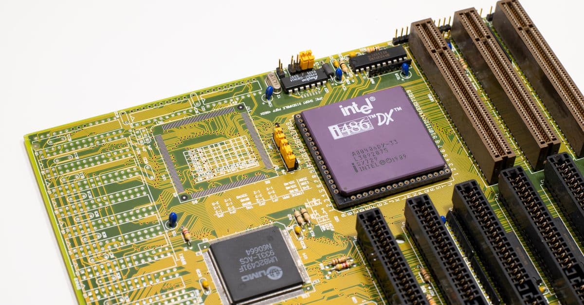
Photo: Jeremy Waterhouse / Pexels
A chip the size of a fingernail is built from up to 100 stacked layers, each patterned with features measured in nanometers and aligned to the layer below with the same kind of precision. One speck of dust can ruin a die, and one misaligned layer can ruin a wafer. The machine that prints the finest layers works with light at a 13.5 nanometer wavelength, which almost everything absorbs. This article walks through why that process is so difficult, where the cost comes from, and why only a few places on Earth can do it at the leading edge.
Key takeaways
- A modern chip can have up to 100 layers and hundreds of process steps, according to chip-equipment maker ASML, and each layer must line up with the others at nanometer precision.
- Extreme ultraviolet (EUV) lithography uses light with a 13.5 nm wavelength. ASML's current machines resolve features down to 13 nm, and its newer High-NA machines to 8 nm.
- Fab air is held to ISO class 1: no more than 10 particles of 100 to 200 nm per cubic meter, versus roughly 10,000 particles in a modern hospital, per ASML.
- Small losses compound. A 99.9 percent success rate per step over 500 steps leaves only about 61 percent of wafers intact.
- TSMC's Arizona program is planned at $265 billion across six logic fabs, two packaging facilities, and an R&D center.
- The 2 nm generation uses nanosheet transistors, and TSMC says its N2 process entered volume production in the fourth quarter of 2025.
What "3nm" actually means
When chipmakers talk about a "3-nanometer" chip, they are not describing a ruler measurement of anything on the die. The names became marketing labels for generations long ago. A "3nm" process is better understood as a generation that packs more transistors into the same area, uses less power, or runs faster than the one before it. That is why comparing node names across companies tells you little.
The names still point to something real. Apple described its A17 Pro as "the industry's first 3-nanometer chip" when it announced the iPhone 15 Pro in September 2023. TSMC says its N2 process, the generation after 3nm, entered volume production in the fourth quarter of 2025 and uses what it calls first-generation nanosheet transistor technology.
A transistor is a tiny electrical switch. A gate electrode controls whether current flows between two terminals, called the source and the drain. Billions of these switches, wired together, make logic circuits and memory. To shrink them, engineers must pack features only dozens of atoms across. A silicon crystal has atoms spaced a fraction of a nanometer apart, so at these sizes the building materials themselves become the limit.
That is where quantum tunneling creeps in. Electrons behave partly like waves, and a wave can leak through a barrier that would stop a ball. In a transistor, thin insulating layers meant to keep current out can leak instead, which wastes power and makes heat. The physics is explained in our piece on quantum tunneling. Every new generation requires new geometries and materials to keep that leakage in check.
From sand to wafer: the starting material
Chips begin as extremely pure silicon. Silicon is extracted from sand-like quartz, purified, grown into a single large crystal, and sliced into thin, disk-shaped wafers roughly the size of a dinner plate. Each wafer is polished until it is flatter than any mirror you own. Hundreds of identical chips, called dies, are patterned across a wafer at the same time, and the wafer is cut apart at the end.
The reason purity and flatness matter is that every later step is a controlled interaction with that surface. A bump, a stray atom, or a crystal flaw gets copied into every layer built on top. Think of building a house of cards on a tablecloth that has lumps in it. The lumps do not matter for the first card, but by the hundredth layer they decide whether the structure stands.
Building a chip in layers: the same loop, again and again
ASML's own overview describes chips as built by "building up layers of interconnected patterns on a silicon wafer." It lists up to 100 layers and hundreds of process steps, with up to four months from the start of manufacturing to a finished chip. The steps fall into a repeating loop:
- Deposit a thin film of material onto the wafer.
- Coat it with a light-sensitive layer called photoresist.
- Expose the photoresist to a pattern of light in a lithography machine.
- Develop and etch, removing material only where the pattern says to.
- Add or modify material, for example by implanting atoms to change how silicon conducts.
- Polish and inspect, flattening the surface and checking the result before the next layer.
Most people picture a chip as a single flat circuit. A better picture is a skyscraper whose floors are built one at a time, where the bottom floors hold transistors and the upper floors hold the wiring that connects them. Each floor needs a different pattern, and each pattern must be lined up with the ones below it. That alignment requirement has a name, overlay, and ASML describes it as needing nanometer precision.
The sequence is not an assembly line in which a wafer travels once from end to end. A wafer re-enters the same machines many times, once per layer. That is one reason fabs are so large and so busy, and why a single machine's downtime can slow an entire factory.
Lithography: drawing with light
The patterning step, photolithography, is the heart of the process. A lithography machine shines light through a pattern (the mask) and projects a shrunken image of it onto the photoresist. Where light hits, the chemistry of the resist changes. Developing the wafer washes away either the exposed or unexposed parts, leaving a stencil for the next step.
The smallest feature a machine can print depends on three things: the wavelength of the light, the numerical aperture of the optics (NA, a measure of how much light the system can gather), and a process factor that engineers call k1. The relationship is usually written as:
Smallest printable feature ≈ k1 × wavelength ÷ NA
A shorter wavelength or a larger NA prints finer detail. For decades, chipmakers used deep ultraviolet (DUV) light at 193 nanometers and squeezed out more detail with clever tricks, including printing a layer in several passes. Eventually, that approach became too slow and too costly for the finest layers, which is why the industry moved to EUV.
EUV and High-NA at a glance
ASML's product pages give these figures:
| System | Wavelength | Numerical aperture | Resolution (ASML figure) |
|---|---|---|---|
| DUV (long-established) | 193 nm | Not listed here | Used for less critical layers |
| EUV (NXE series) | 13.5 nm | 0.33 | 13 nm |
| High-NA EUV (EXE series) | 13.5 nm | 0.55 | 8 nm |
You can check the table with the formula above. Using 13 nm, 0.33, and 13.5 nm, the implied k1 is about 0.32. Using 8 nm, 0.55, and 13.5 nm, it comes out about the same, around 0.33. Higher NA, not a shorter wavelength, accounts for the jump from 13 nm to 8 nm. ASML says its NXE:3800E supports high-volume manufacturing of 2 nm-class logic and leading-edge memory, and that EXE:5000 is the first in a new generation. Our deeper article on EUV lithography covers the machine itself.
An important detail is that chips do not use only EUV. According to ASML, EUV handles the most critical layers with the smallest features, while DUV machines handle the less critical layers with larger features. A single chip is a hybrid of both.
Why EUV is so strange
EUV light has a wavelength of 13.5 nanometers, far shorter than the visible light our eyes use. At that wavelength, almost everything absorbs light, including glass and air. Two consequences follow.
First, a conventional lens cannot work. Glass would absorb the light, so EUV systems use mirrors instead, coated with many thin alternating layers that reflect a narrow band of the light. Each reflection still loses some of it, so the whole optical path is a game of conserving a scarce resource.
Second, the beam must travel in vacuum. Air would absorb it. The whole system, from the light source to the wafer, is therefore sealed in a vacuum environment.
Generating the light is its own engineering story. In the standard approach, a powerful laser hits tiny droplets of molten tin, which turn into a hot plasma that radiates at 13.5 nm. The light is then collected and sent through the optics. The pulses have to be repeated very rapidly and each one has to deliver the same amount of light, because the dose reaching the wafer determines how the photoresist reacts.
The wafer stage's job is just as demanding. It must move the wafer, stop it, and line it up to nanometer precision, over and over. It is a bit like landing a plane on a moving ship repeatedly, except the margin for error is a few atoms wide.
The cleanroom: why a speck of dust is a disaster
At nanometer scales, a particle that would be invisible to the naked eye can be a boulder. A speck landing on a wafer can block light during exposure, cause a wiring break, or short two lines together. The defense is the cleanroom.
ASML says fab cleanrooms meet ISO class 1, which permits no more than 10 particles of 100 to 200 nanometers per cubic meter and none larger than 200 nm. It describes fab air as about 10,000 times cleaner than outside air, and notes that a modern hospital has about 10,000 dust particles per cubic meter. Robots move wafers between machines, because people shed skin and fibers.
This sets the practical limits of the whole enterprise. Every material that enters, every gas, and every liquid has to be filtered, monitored, and tested. Part of the huge expense of a fab is not the glamorous machines but the air handling, the water purification, and the monitoring that keep the environment stable.
Why small errors compound: the yield problem
Manufacturers talk about yield: the fraction of chips on a wafer that work. Yield is where the physics turns into money, because a wafer costs nearly the same to process whether 90 percent of its chips work or 30 percent do.
Two effects make yield hard. The first is that errors compound across steps. The table below is an illustration, not a measurement from any real factory. It assumes that each step has an independent chance of ruining a wafer and that there are 500 steps, a number consistent with ASML's "hundreds of steps."
| Per-step success rate | Wafers surviving 500 steps |
|---|---|
| 99 percent | about 0.7 percent |
| 99.9 percent | about 61 percent |
| 99.99 percent | about 95 percent |
The arithmetic is simple: multiply the success rate by itself 500 times. A process that sounds excellent at 99 percent per step would be useless. The industry's task is to push every step to a level of reliability that most manufacturing never sees.
The second effect concerns die size. A larger chip has more surface area for a random defect to hit. A common simplified model says the chance a die escapes defects is e raised to the power of minus the area times the defect density. The numbers below use an assumed, illustrative density of 0.1 defects per square centimeter.
| Die area | Estimated yield |
|---|---|
| 1 cm² | about 90 percent |
| 2 cm² | about 82 percent |
| 6 cm² | about 55 percent |
| 8 cm² | about 45 percent |
This is why very large chips, such as the biggest AI accelerators, are expensive, and part of the motivation for chiplets: stitching several small dies together can be cheaper than risking one huge die. A defect then kills only a small piece, not an entire big chip. Real yield models are more elaborate, and real defect densities are closely guarded, but the logic holds.
The new transistor shape: from fins to nanosheets
As transistors shrank, the old flat design leaked too much current. The industry moved to a three-dimensional design called the FinFET, in which the channel rises like a fin and the gate wraps around three sides. The next step wraps the gate around the channel on all sides. TSMC calls its version nanosheet transistor technology; Intel has used the name RibbonFET for a similar approach. Stacks of thin horizontal sheets of silicon pass through the gate, giving finer control over the electrons.
The reason this matters is control. A good gate is like a good faucet handle: it should shut the flow completely when off and open it freely when on. At very small sizes, a handle that touches only part of the pipe lets a trickle through even when closed. Surrounding the channel more completely shuts the trickle.
TSMC's N2 page says volume production began in the fourth quarter of 2025 as planned. Beyond this step, researchers explore stacking transistors on top of each other and new channel materials, each of which adds new deposition and etching problems. To see where the transistor story started, read how the transistor changed everything and the history of the invention of the microchip.
The cost: why a single fab runs into the billions
The machines are not the only expense. The building, the cleanroom, the utilities, the hundreds of tools, and years of training for operators all add up. The TSMC Arizona program offers a concrete case study. According to TSMC's Arizona page, the planned total investment has grown from an original $12 billion to $265 billion. Current plans include six semiconductor logic wafer fabs, two advanced packaging facilities, and an R&D center. TSMC describes it as the largest foreign direct investment in a greenfield project in United States history.
| Facility | Process | Milestone per TSMC |
|---|---|---|
| Fab 1 | N4 | High-volume production began in Q4 2024 |
| Fab 2 | N3 | Structure completed in 2025; volume production targeted for second half of 2027 |
| Fab 3 | N2 and A16 | Groundbreaking April 2025; volume production targeted by the end of the decade |
| Fab 4 and first packaging fab | Not specified | Initial construction started in early 2026; no production date given |
The table makes a point that the headline dollar figure can hide. Even for the world's leading contract manufacturer, which already knows how to do this, a new site takes years to go from construction to volume output. TSMC also says that in July 2026 it announced intent to build several more logic fabs for 2 nm and below, plus advanced packaging fabs.
Governments have responded with subsidies. According to the National Institute of Standards and Technology's CHIPS page, the CHIPS and Science Act provided $50 billion, including $39 billion for manufacturing incentives and $11 billion for research and development. Money, however, does not make a fab. Fabs also need engineers, suppliers, water, and electricity, and all of those take time to assemble.
Why a few places dominate
Making a chip is a team sport. Chemical suppliers, wafer makers, equipment makers, software tool vendors, and test houses all have to be good at once. A change in one affects the others, so the system rewards places that already have the whole web in place. This produces geographic concentration: the more the cluster knows, the easier it is for the next fab to be built nearby.
The concentration shows up at several levels. At the tool level, EUV machines come from a single supplier, ASML, and each depends on specialized parts such as mirrors made by a partner. At the factory level, only a handful of companies can produce the most advanced logic. At the regional level, much of that capacity is in East Asia. The exact shares change, and Specific percentages are left out because sources disagree on definitions, such as what counts as "advanced." Our ranking of countries that produce the most semiconductors lays out the national data in more detail.
The result is a supply chain in which a single disruption can ripple widely. The pandemic-era chip shortage, which hit automakers and consumer electronics makers among others, showed how little slack there was. Widely reported accounts say automakers had cut orders when demand seemed weak and then found themselves at the back of the line when demand returned, since chipmakers had reallocated capacity to customers who kept ordering. Similar dependency issues appear in other advanced manufacturing; for a parallel in factory automation, see countries with the most industrial robots per worker.
Taiwan's role is the point policymakers worry about most, because a large part of leading-edge capacity sits on one island in a contested region. Forecasts are outside the scope of this article. The engineering point is that duplicating a cluster takes many years, as the Arizona timeline shows, so risk cannot be reduced quickly.
Common misconceptions
"Chips are made by printing tiny circuits, like a printer." Lithography does resemble printing, but the circuit only appears after dozens of deposit, etch, and polish steps. Light creates the stencil; chemistry and machines do the building.
"Whoever has the best machines wins." Machines matter, but so do process know-how and yield. Two factories with identical tools can have very different yields, because the recipe, the cleanliness, and thousands of tuning decisions differ. Buying equipment does not buy experience.
"A smaller node number always means a faster chip." Node names are labels, and a chip's speed and power also depend on design, memory, packaging, and software. Larger designs on older nodes remain important for cars, appliances, and industrial equipment.
"We can just build more fabs." Fabs can be built, but not quickly. The Arizona timeline runs from groundbreaking to production over several years, and every step depends on suppliers who also have to expand. Even then, the first production runs have to be tuned to reach good yield.
"It is only a silicon story." Silicon is the base, but modern chips use many materials, including metals for wiring and insulating films, each with its own purity and deposition challenge. Fabs are as much a chemistry business as a physics one. For another case of a prized material whose price reflects scarcity and processing, see why gold is so expensive.
What this means
The difficulty of semiconductor manufacturing is not a single hard problem. It is a stack of hard problems that all have to be solved at once: light that gets absorbed by air, layers that must align to nanometers, a cleanroom thousands of times cleaner than a hospital, and a yield equation that punishes even tiny error rates. Each is manageable alone. The combination, repeated hundreds of times on every wafer, is what limits the number of companies that can do it and the speed at which new capacity appears.
That also explains the shape of the industry. Billions of dollars, years of construction, and a whole supplier ecosystem make new entrants rare and new fabs slow. For anyone reading a headline about a chip shortage or a new fab, the useful question is how long the lead time is and how many other pieces have to be in place. The same logic holds for other precision-crafted goods, as in why silk is so expensive, and for devices that depend on chips, such as VR and AR headsets. For the factory-floor view of the same process, see how semiconductor fabs work, and for the step-by-step version, how semiconductors are made.
Frequently Asked Questions
Q: What does "3nm" mean in a chip? A: It is a name for a manufacturing generation, not a measurement of any one feature. A 3nm-class process packs more transistors per area and uses less power than the generation before. Apple called the A17 Pro the first 3-nanometer chip in 2023, and TSMC's following generation, N2, entered volume production in the fourth quarter of 2025.
Q: Why is EUV lithography so difficult? A: EUV light has a 13.5 nm wavelength, and almost everything absorbs it, including glass and air. That forces the machine to use mirrors in a vacuum and an exacting plasma light source. ASML's current EUV machines resolve 13 nm features, and High-NA machines resolve 8 nm.
Q: How many steps does it take to make a chip? A: ASML describes hundreds of process steps and up to 100 layers per chip, with up to four months from the start of manufacturing to a finished chip. Each layer needs a pattern aligned to the ones below it at nanometer precision, which is why the process is so sensitive to errors.
Q: Why do fabs need cleanrooms? A: At nanometer scale, a speck of dust can destroy a circuit. ASML says fab cleanrooms meet ISO class 1, allowing no more than 10 particles of 100 to 200 nm per cubic meter, about 10,000 times cleaner than outside air. A modern hospital has about 10,000 dust particles per cubic meter.
Q: How much do new chip factories cost? A: Costs run to billions of dollars. TSMC says its Arizona program has grown from an original $12 billion to a planned $265 billion, covering six logic fabs, two advanced packaging facilities, and an R&D center. The total is a multi-site program, not the cost of a single building.
Q: Why not simply build more fabs outside Asia? A: Fabs can be built elsewhere, and governments are funding them. The CHIPS and Science Act provided $50 billion in the United States. The barriers are time and ecosystem: TSMC's Arizona timeline runs from groundbreaking to volume production over several years, and suppliers, engineers, and utilities must scale alongside.
Sources
- ASML, "How microchips are made": https://www.asml.com/en/technology/all-about-microchips/how-microchips-are-made
- ASML, "EUV lithography systems": https://www.asml.com/en/products/euv-lithography-systems
- TSMC, "N2 technology": https://www.tsmc.com/english/dedicatedFoundry/technology/logic/l_2nm
- TSMC, "TSMC Arizona": https://www.tsmc.com/static/abouttsmcaz/index.htm
- NIST, "CHIPS for America": https://www.nist.gov/chips
- Apple Newsroom, "Apple unveils iPhone 15 Pro and iPhone 15 Pro Max," September 2023: https://www.apple.com/newsroom/2023/09/apple-unveils-iphone-15-pro-and-iphone-15-pro-max/
Related Reading
- Countries That Produce the Most Semiconductors (2025)
- Why Gold Is So Expensive — The Chemistry and Economics Behind the World's Most Coveted Metal
- What Are VR and AR — and Where Is the Metaverse Actually Going?
- Countries With the Most Industrial Robots Per Worker (2025)
- Why Silk Is So Expensive — The Ancient Biology Behind the World's Most Coveted Fabric
Follow new articles
Add SciHub101 to your feed reader to see new science and technology stories.
About the Author
SciHub101 is an independent science and technology publication founded and edited by Buğra Sözeri, a software engineer and app developer based in Türkiye. AI tools assist with drafting and research. Source documentation in the existing archive is uneven, and articles are being reviewed and corrected. The Editorial Team byline identifies editorial responsibility; it does not certify specialist or independent human review. Where we compare products, anything built by our own team is labelled as such — see the editorial guidelines and About page for how corrections and disclosures work.
Related Articles

How Do Quantum Computers Actually Work? Beyond the Hype
Quantum computers don't replace your laptop — they solve a small set of problems exponentially faster. Here's what they really are, why they're hard to build, and what they'll change.

How Misinformation Spreads Online — And What Actually Stops It
False information can travel faster than truth on social media. This is a predictable result of how people and platforms behave. Here is what the research says about why it spreads and which fixes have evidence behind them.
Countries That Produce the Most Semiconductors (2026)
Taiwan held 92% of the world's most advanced chip capacity in a 2021 study, South Korea dominates memory, and one Dutch company makes the only EUV lithography machines. Who controls which layer of the chip supply chain, with sourced figures.
Semiconductor Chips: How They Work
A modern processor packs tens of billions of transistors onto a sliver of silicon. Here is how doped silicon becomes switches, switches become logic, and logic becomes a computer.
Complete Technology Guide 2026 — How Modern Tech Works
The complete guide to technology in 2026: how the internet, semiconductors, and quantum computing work, AI hardware, cybersecurity, and what's coming next.
Countries with the Most Robots in Manufacturing (Robot Density Ranked)
South Korea has 1,012 industrial robots per 10,000 manufacturing workers — the highest robot density ever recorded for a major economy. That is more than six times the global average of 162, and more than double Germany's figure. The IFR World Robotics 2024 report shows a world where automation in factories is accelerating faster than at any point in industrial history.