How Camera Sensors Work — CCD vs CMOS
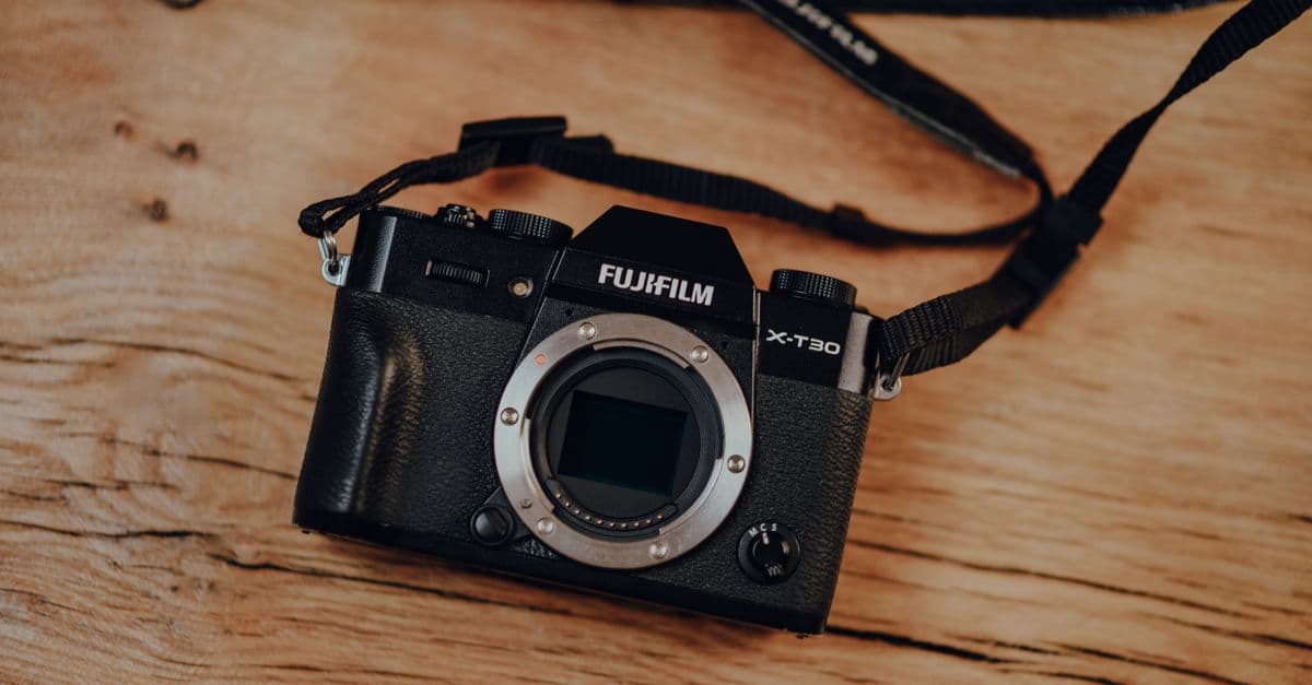
Photo: Grish Petrosyan / Pexels
Every digital photograph begins as a pile of counted electrons. A camera sensor is a slab of silicon divided into millions of tiny wells, and each well tallies how many photons landed on it during the exposure. Color, noise, low-light ability, and the gap between a phone and a full-frame camera all follow from that counting problem. This article explains how camera sensors work, how CCD and CMOS designs read the counts out, why pixel size matters more than megapixels, and what burst-stacking software adds on top.
How a photodiode turns light into a number
A sensor is a dense array of photodiodes, small semiconductor structures that convert light into electric charge. The mechanism is the photoelectric effect: a photon with enough energy knocks an electron loose from a silicon atom. Einstein's explanation of that effect earned him the 1921 Nobel Prize in Physics, and the photoelectric effect experiment is still the cleanest demonstration that light arrives in discrete packets. (For the particle itself, see our explainer on what a photon is.)
Think of a field of buckets set out in a rainstorm. Each photodiode is a bucket, each photon is a raindrop, and the exposure is the time the buckets stay out. When the shutter closes, the camera does not ask how hard it rained. It asks how many drops landed in each bucket. The electrons collect in a potential well, a region of the silicon where an electric field holds them in place until readout.
Readout converts that charge into a voltage, and an analog-to-digital converter (ADC) turns the voltage into an integer. Raw files from many cameras store 12 or 14 bits per pixel, which means 4,096 or 16,384 possible levels per photosite. The response is roughly linear: twice the photons, twice the number. That linearity is why raw files look dark and flat until software applies a tone curve.
Two limits matter from the start. Every well can hold only so many electrons, a ceiling called the full-well capacity, and once a pixel fills, extra light is thrown away and the highlight clips to white. And not every photon produces an electron. The fraction that does is the quantum efficiency, which rises when engineers keep wiring and reflections out of the light path (more on that below).
Silicon also has a built-in blind spot. Its bandgap, about 1.12 electron-volts, means photons with wavelengths beyond roughly 1,100 nanometers cannot free an electron. Long before that cutoff, though, silicon responds to near-infrared light that human eyes cannot see, which is why camera makers put an infrared-blocking filter in front of the sensor. Without it, a leaf can render as a pale ghost and black fabric can turn purple.
The detail that surprises people: a photodiode does not record brightness or color. It records a count of electrons. Everything you think of as an image is arithmetic done on counts.
Why every pixel sees only one color
Silicon does not know what color a photon was. A photon of 450 nanometers and one of 650 nanometers each free one electron, and the well cannot tell them apart. So a bare sensor produces a monochrome picture. Color has to be added with a filter array laid over the pixels.
Almost every camera uses a Bayer filter array, invented by Bryce Bayer at Eastman Kodak. US Patent 3,971,065, titled "Color imaging array," was filed on March 5, 1975, and granted on July 20, 1976. Bayer's design puts green-sensitive elements at every other position, so they make up half the array, and fills the remaining positions with red and blue in alternating rows. Photographers shorthand the repeating 2×2 tile as RGGB: one red, two green, one blue.
The logic is borrowed from vision. In Bayer's patent, the green elements stand in for luminance, the brightness detail that human sight is most sensitive to, while red and blue carry chrominance, the color information that our eyes resolve more coarsely. If you want to see why the eye treats these channels so differently, our piece on how the human eye works walks through rods, cones, and the retina.
What demosaicing guesses
Each pixel therefore knows one number: how much red, green, or blue light reached it. The other two values at that location are missing. Software fills them in by looking at neighbors, a step called demosaicing. It is closer to educated reconstruction than to measurement. Two thirds of the color values in a typical photograph are interpolated.
Think of a paint-by-number picture where every cell is labeled with a single color, and you must infer the full-color painting by looking at the cells around each one. In smooth areas the guess is easy. At sharp edges, such as a black power line against a white sky, a simple algorithm can invent false colors or a zipper-like pattern. Better algorithms detect edge direction first and interpolate along the edge rather than across it.
Regular patterns cause a second problem: moiré, the shimmering bands you see when a fine pattern such as a tight fabric weave beats against the sensor's grid. Traditional cameras put an optical low-pass filter in front of the sensor to blur the image very slightly and suppress moiré, at a small cost in sharpness.
Three ways to get color out of silicon
| Design | How it works | Strength | Trade-off |
|---|---|---|---|
| Bayer (RGGB) | 2×2 tile of one red, two green, one blue filter; missing colors interpolated | Simple, cheap, well understood; used in almost all cameras | Needs demosaicing; regular grid invites moiré |
| Fujifilm X-Trans | 6×6 pseudo-random tile with 20 green, 8 red, and 8 blue photosites; introduced with the X-Pro1 in 2012 | Every row and column holds all three colors; less need for a low-pass filter | Harder demosaicing; needs more processing |
| Foveon X3 | Three stacked photodiode layers per pixel; blue absorbed near the surface, red deepest | Full color at every location, no demosaicing | Color separation by depth is imperfect; noisier at high ISO |
The Foveon X3 sensor, first used in Sigma's SD9 DSLR in 2002, works because silicon absorbs short wavelengths near the surface and long wavelengths deeper in. PVEducation notes that blue light is absorbed within a few microns of the surface, while red is absorbed so weakly that some of it passes through even a few hundred microns of silicon. The Foveon's stack is under five micrometers thick in total, so the deepest layer cannot perfectly isolate red. Wikipedia's summary of the design reports that the cross-contamination between layers hurts color accuracy and that the matrix math to unmix them can amplify color noise in low light. As of 2025, no Sigma camera on sale uses it.
For a related look at what happens after the sensor, see how digital cameras capture color and our explainer on digital color spaces.
CCD vs CMOS: two ways to empty the buckets
Once the exposure ends, the charge in millions of wells has to be carried to an amplifier and a converter. The two sensor families differ mainly in how they do this.
A CCD (charge-coupled device) moves the charge itself. The device is a row of linked capacitors, and under the control of external clock signals each capacitor passes its charge packet to its neighbor, like a bucket brigade passing water hand to hand until the last person pours it into a single measuring cup at the edge. The IEEE milestone entry dates the invention at Bell Labs to October 17, 1969, and credits Willard Boyle, George Smith, and Michael Tompsett. It notes that the CCD was originally conceived for digital memory, then proved better suited to capturing light. Boyle and Smith shared the 2009 Nobel Prize in Physics for the invention.
Because every charge packet passes through the same output amplifier, a CCD produces very uniform, low-noise images. The price is speed, power, and manufacturing cost: the whole sensor must be clocked, and the process is specialized.
A CMOS (complementary metal-oxide-semiconductor) sensor puts an amplifier in every pixel, so the voltage can be read directly from each row and column without shifting charge across the chip. The design was developed into a practical "camera on a chip" by Eric Fossum and his team at NASA's Jet Propulsion Laboratory in the early 1990s. According to JPL's 2017 news release on the Queen Elizabeth Prize, the team was trying to shrink the size and power of spacecraft cameras, and the resulting CMOS active-pixel sensor needed about 1 percent of the power of the earlier CCDs. Fossum co-founded Photobit in 1995 to commercialize the technology.
Early CMOS sensors were noisier than CCDs, and giving every pixel its own amplifier invites pixel-to-pixel variation that a single shared amplifier avoids. A key fix was the pinned photodiode, invented at NEC in 1980 by Nobukazu Teranishi and colleagues, which reduced lag and dark current. According to Wikipedia's image sensor article, the pinned photodiode went into most CCDs from 1987 and has been used in nearly all CCD and CMOS sensors since. The same source reports that CMOS sales passed CCD sales by 2007.
| Feature | CCD | CMOS |
|---|---|---|
| How charge leaves the chip | Shifted pixel to pixel to a few output amplifiers | Converted to voltage inside each pixel |
| Readout speed | Slower; whole array is clocked | Fast; rows can be read in parallel |
| Power draw | High | Low (JPL reported about 1% of CCD power for its spacecraft sensor) |
| On-chip electronics | Minimal | ADCs, memory, and processing can share the chip |
| Typical shutter | Global (all pixels exposed together) in many designs | Rolling by default; global needs extra storage circuits |
| Today's role | Specialized science and astronomy | Phones, mirrorless cameras, DSLRs, video |
CCDs have not vanished. The European Space Agency's Gaia spacecraft carries 106 CCDs with almost one billion pixels in total, covering 0.38 square meters, which ESA calls the largest focal plane ever flown in space. When the goal is measuring the positions of about one billion stars with extreme uniformity, the CCD's even response is worth the cost. For how space telescopes handle other wavelengths, see how space telescopes see in infrared.
Why pixel size beats megapixel count
If you remember one idea about sensors, make it this: each pixel is a bucket, and a bigger bucket catches more rain. The reason that matters is statistical.
Light arrives randomly. Even a perfectly steady lamp delivers photons with a scatter that follows Poisson statistics, so if a pixel collects N electrons on average, the random fluctuation (the shot noise) is the square root of N. The signal-to-noise ratio (SNR) is signal divided by noise, which works out to the square root of N as well. This noise is not a manufacturing flaw. It is built into light itself, which is why no sensor can escape it.
A worked example makes the stakes concrete. Suppose a pixel collects 10,000 electrons in a given exposure. Shot noise is 100 electrons and the SNR is 100, or 40 decibels. Now take a pixel with one twentieth of the area, under the same lens, the same scene, and the same exposure. It collects about 500 electrons, so the shot noise is about 22 electrons and the SNR is about 22. Twenty times less area costs roughly 4.5 times in SNR, since the square root of 20 is about 4.5.
Read noise is the second source. It is added when the analog signal is amplified and converted to a digital number, and it does not depend on how much light arrived. In bright scenes, shot noise dominates and read noise hardly matters. In dim scenes, where each pixel holds only a handful of electrons, read noise can swamp the signal, and this is where good sensor design earns its reputation.
How sensor formats compare
The table below uses nominal sensor dimensions and divides area by pixel count, so the pitch figures are computed estimates that ignore the gaps between pixels. Pixel pitch is the center-to-center distance.
| Format | Nominal size (mm) | Area (mm²) | Area vs phone | Pitch at 12 MP | Typical use |
|---|---|---|---|---|---|
| Phone, 1/1.7-inch | 7.6 × 5.7 | 43 | 1.0× | about 1.9 µm | Flagship phone cameras |
| 1-inch | 13.2 × 8.8 | 116 | 2.7× | about 3.1 µm | Premium compacts |
| Micro Four Thirds | 17.3 × 13 | 225 | 5.2× | about 4.3 µm | Olympus/OM System, Panasonic |
| APS-C | 23.5 × 15.6 | 367 | 8.5× | about 5.5 µm | Fujifilm X, Sony α6000 series |
| Full frame | 36 × 24 | 864 | 19.9× | about 8.5 µm | Sony α7, Canon R, Nikon Z |
| Medium format | 44 × 33 | 1,452 | 33.5× | about 11 µm | Hasselblad, Fujifilm GFX |
The comparison shows why a 61-megapixel full-frame sensor, with a pitch near 3.8 µm, has pixels about the size of those on a 12-megapixel Micro Four Thirds camera. It also shows the phone's handicap: at equal pixel counts, each phone pixel sees roughly one twentieth of the light that a full-frame pixel sees.
How pixel binning works around the problem
Phone makers answer with pixel binning: combining neighboring pixels so that the sensor acts like a smaller number of larger ones. Samsung's 200-megapixel ISOCELL HP2 has 0.6 µm pixels on a 1/1.3-inch sensor, and it merges 16 pixels into one 2.4 µm pixel for a 12.5-megapixel image, or four into one 1.2 µm pixel for 50 megapixels. Sony's IMX989, the 1-inch sensor in the Xiaomi 12S Ultra, has 50.3 megapixels at 1.6 µm per pixel and bins to 3.2 µm in its Quad-Bayer design.
Binning trades resolution for light. A 200-megapixel label describes the grid, not the typical output. Most shots from such a phone are 12.5 or 50 megapixels, because that is where the signal-to-noise ratio is acceptable.
Sensor area, not pixel pitch alone, sets the total light for the whole frame. Framing the same scene with the same f-number, a larger sensor gathers more total light because it spans more of the image the lens projects. This is the physical reason dedicated cameras keep their edge in dim rooms.
When more pixels stop helping: the diffraction limit
There is a second reason megapixel counts mislead, and it comes from the lens. Light passing through a circular aperture does not focus to a point. It forms a small bullseye called an Airy disk, and the diameter of its bright center is about 2.44 × wavelength × f-number. For green light at 550 nanometers (0.55 µm), here is how that plays out:
| Lens aperture | Airy disk diameter | Meaning |
|---|---|---|
| f/1.8 (typical phone main lens) | about 2.4 µm | Spot spans about two 1.2 µm pixels across |
| f/2.8 | about 3.8 µm | Close to a 61 MP full-frame pixel pitch |
| f/8 | about 10.7 µm | Wider than the 12 MP pixel pitch of every format in the format table, medium format excepted |
The numbers come from a standard optics formula, not from any one manufacturer's tests. They show that a 0.6 µm pixel behind an f/1.8 phone lens samples far finer than the lens can resolve. The extra pixels still help with demosaicing and noise averaging, but they do not add real detail beyond what the optics deliver. Stopping a full-frame lens down to f/8 or beyond blurs the image at the pixel level on a high-resolution sensor for the same reason.
So the real constraints are layered: the lens resolves up to a limit, the pixel grid samples up to a limit, and noise limits what you can recover from either. Doubling any one of them without the others does little.
What ISO, dynamic range, and bit depth really mean
ISO is usually described as sensitivity, but the photodiodes do not become more sensitive when you turn the dial. Raising ISO applies more amplification to the signal between the photodiode and the ADC (analog gain), sometimes followed by a digital multiplication. Amplification scales the signal and the noise together. What changes is the exposure you need: at higher ISO, the camera can output a bright image from fewer photons, but those fewer photons carry the same relative shot noise, so the image looks grainier.
Dynamic range is the ratio between the brightest signal a pixel can hold before clipping and the faintest signal that stands above the noise floor. Photographers measure it in stops, where each stop is a factor of two. DXOMark measured the 61.2-megapixel back-illuminated CMOS sensor in the Sony A7R IV at 14.8 EV of dynamic range at base ISO 100. Since 2 raised to the power 14.8 is about 28,000, that sensor spans a brightness ratio near 28,000 to one in a single exposure, normalized by DXOMark's methodology.
This is where bit depth connects. A 12-bit raw file has 4,096 levels, and a 14-bit file has 16,384. Because the response is linear, a 14-bit file can in principle encode about 14 stops, so the file format must have enough levels to hold what the sensor can distinguish.
The practical limits show up in two places. Highlights clip abruptly when a well fills. Shadows dissolve gradually into noise. That asymmetry explains why the burst method described below deliberately underexposes each frame: a dark frame can be brightened and averaged, but a clipped highlight cannot be recovered.
How back-illuminated, stacked, and global-shutter sensors changed the chip
Early CMOS pixels had a layout problem: the photodiode sat underneath layers of metal wiring, so some light was blocked or scattered before it reached silicon. In a back-side illuminated (BSI) sensor, the silicon is flipped and thinned so light enters from the back, directly into the photodiode, while the wiring lies behind it. Sony announced its Exmor R back-illuminated CMOS technology on June 11, 2008, with a five-megapixel prototype. DPReview's coverage reports that the TX1 and WX1 compacts were the first products to use it, and that Sony claimed nearly twice the sensitivity of a conventional front-illuminated CMOS sensor (a gain of 6 decibels) plus about 2 decibels less random noise. The benefit is largest in small pixels, where wiring would otherwise eclipse a big fraction of the opening.
The next step moved the processing circuitry off the pixel layer entirely. A stacked sensor bonds the photodiode wafer to a separate logic wafer, so the pixels get the full area for light collection while memory and processors sit directly underneath. Sony introduced its Exmor RS stacked CMOS sensors in 2012. Stacking enables fast readout and room for on-chip memory, which later made possible the burst speeds and in-sensor autofocus processing of current cameras.
Why rolling shutters warp moving subjects
Most CMOS sensors use an electronic rolling shutter: each row's exposure immediately precedes its readout, so the readout wave sweeps from top to bottom across the frame. If the subject or camera moves during that sweep, the top and bottom of the image record different moments, and a propeller bends or a building leans during a fast pan. A global shutter exposes and reads every pixel at the same moment, which requires extra storage circuitry in each pixel to hold the charge until readout. According to Wikipedia's discussion of image sensors, that extra circuitry is the reason global shutters are less common.
Stacking changed the economics. Sony's Alpha 9 III, announced on November 7, 2023, was reported by Newsshooter as the first full-frame camera with a global shutter sensor. It uses a roughly 24.6-megapixel stacked CMOS sensor, shoots up to about 120 frames per second without blackout, and reaches a top shutter speed of 1/80,000 second (1/16,000 second in continuous bursts). A long-standing CCD advantage has arrived in mainstream CMOS, at a price: the camera's resolution is modest, and the storage in each pixel takes space that could hold more light.
How phones borrow light from many frames
A phone sensor cannot match a full-frame sensor's raw collection of light, but it can take many exposures in the time it takes a photographer to take one. The best-documented method is Google's HDR+, described by Sam Hasinoff and colleagues at SIGGRAPH Asia in 2016.
Instead of bracketing exposures, HDR+ captures a burst of frames at a constant, short exposure, deliberately low enough to protect the highlights. The pipeline starts from raw Bayer data rather than from the phone's finished image, which preserves more bits per pixel and avoids premature tone mapping. It then aligns the frames with an FFT-based algorithm and merges them with a hybrid 2D/3D Wiener filter, which weighs each pixel by how well it matches the reference. In the paper, a 12-megapixel result took about four seconds on the phone.
The statistics are the same as for pixel size. Averaging N aligned frames of the same scene reduces random noise by about the square root of N. Averaging nine frames cuts noise to a third. In effect, nine short exposures stand in for one that is nine times longer, without the blur of a long handheld exposure. Because the frames are short, bright areas do not clip, and the shadows are lifted by combining many noisy samples.
Think of a crowd of nine people sketching the same face with shaky hands. Any one sketch is wobbly, but if you overlay all nine and keep what they agree on, the lines come out clean. The aligned merge is the overlay, and the Wiener filter decides where the sketches agree.
Burst photography has limits. A fast-moving subject can differ between frames, so the merge must reject or blend those regions, and errors appear as ghosting or smeared textures. Handheld shake larger than the alignment can handle also breaks the match. Newer systems add machine-learning models for denoising, demosaicing, and segmentation, which depend on the same sort of parallel hardware that powers GPUs and, increasingly, on-device models like those described in our look at edge AI on phones. Generative systems built on diffusion models go further, and they raise a question the sensor never had to answer: how much of the final picture was recorded, and how much was inferred?
What people get wrong about camera sensors
"More megapixels means a better camera." Resolution is one number among several. At a fixed sensor size, more pixels means smaller ones, so each collects less light. Whether that matters depends on the lens, the output size, and the light level, and more pixels only pay off when the lens and the viewing size can use them.
"Raising ISO makes the sensor more sensitive." It amplifies what the sensor captured. The only way to capture more signal is a bigger aperture, a longer exposure, a larger sensor, or a more efficient design.
"CCD sensors have better color." CCDs were known for uniform, low-noise output in early digital cameras, which gave them a reputation. But color in a Bayer camera comes from the filter array and the processing, not from whether the charge is read out by bucket brigade or by per-pixel amplifiers. Modern back-illuminated CMOS sensors match or exceed CCD noise performance while using far less power.
"Phone cameras fake detail." Computational photography combines real photons from several exposures. That is measurement, not invention, though the line blurs when systems add learned priors about what faces or text should look like. The honest framing is that phones trade fidelity to a single moment for fidelity to the scene as a whole.
"Sensor size alone decides quality." Size sets the ceiling on total light, but the lens, the sensor's quantum efficiency, read noise, and the processing pipeline all shape the result. A sensor with a better design and a smarter pipeline can narrow the gap with a larger but older one.
For the history that led here, from camera obscura to digital sensors, see our camera invention timeline.
The takeaway
A camera sensor is a statistics instrument disguised as a picture-taker. It counts electrons, and because counting random arrivals has a built-in error, the quality of an image depends on how many counts each pixel collects, which depends on area, light, and time. Every clever step in the chain, from the Bayer filter to back-side illumination to burst merging, is a way of collecting more counts, or of squeezing a cleaner estimate out of the counts available.
That is also why the spec sheet misleads. Megapixels describe how finely the grid slices the image, not how much light each slice receives. When you compare cameras, ask about sensor area, pixel pitch, and how the camera combines frames, and you will predict real-world results better than the headline number can.
FAQ
Q: Are more megapixels always better? A: No. On the same sensor size, more megapixels means smaller pixels with less light each, so noise per pixel rises. Extra resolution helps only if the lens can resolve it and you print very large or crop heavily. Many phone cameras bin pixels to 12.5 or 50 megapixels for this reason.
Q: Why are phone cameras so good despite tiny sensors? A: They combine many short exposures into one image, a method documented in Google's HDR+ paper. Averaging N frames reduces random noise by about the square root of N, and software handles alignment, tone mapping, and denoising. The trade-off is heavy processing and less raw flexibility than a larger sensor offers.
Q: Is CCD obsolete? A: For consumer cameras, yes. CMOS sales passed CCD sales by 2007, and phones, mirrorless cameras, and DSLRs all use CMOS. CCDs persist where uniform response matters more than cost or speed, as in ESA's Gaia spacecraft, which carries 106 CCDs.
Q: What is back-side illumination (BSI)? A: A CMOS design that flips and thins the silicon so light reaches the photodiode directly rather than passing through the wiring layer. Sony announced its Exmor R BSI technology in June 2008. It helps most in small pixels, where wiring would block a large share of the opening.
Q: Why do videos look wobbly on fast pans? A: Rolling shutter. Rows are read out in sequence from top to bottom, so the bottom of the frame is captured slightly later than the top. A global shutter, as in Sony's Alpha 9 III, exposes all pixels at once and removes the effect.
Q: Does a bigger sensor always mean a better photo? A: It raises the ceiling on light collection for the same framing and f-number, which lowers noise. But lens quality, sensor efficiency, and software also count. A recent small sensor with good processing can beat an older large one.
Sources
- Hasinoff, S. W., Sharlet, D., Geiss, R., Adams, A., Barron, J. T., Kainz, F., Chen, J., and Levoy, M. (2016). Burst photography for high dynamic range and low-light imaging on mobile cameras. SIGGRAPH Asia.
- Bayer, B. E. (1976). Color imaging array, US Patent 3,971,065. Eastman Kodak.
- IEEE Milestones: Charge-Coupled Device, 1969.
- NASA Jet Propulsion Laboratory (2017). Queen Elizabeth Prize honors digital imaging pioneers.
- European Space Agency. Inside Gaia's billion-pixel camera.
- DXOMARK. Sony A7R IV sensor review.
- PVEducation. Absorption depth.
- Newsshooter (November 7, 2023). Sony Alpha 9 III has world's first full-frame global shutter sensor.
Follow new articles
Add SciHub101 to your feed reader to see new science and technology stories.
About the Author
SciHub101 is an independent science and technology publication founded and edited by Buğra Sözeri, a software engineer and app developer based in Türkiye. AI tools assist with drafting and research. Source documentation in the existing archive is uneven, and articles are being reviewed and corrected. The Editorial Team byline identifies editorial responsibility; it does not certify specialist or independent human review. Where we compare products, anything built by our own team is labelled as such — see the editorial guidelines and About page for how corrections and disclosures work.
Related Articles
Electric Cars vs Gas Cars — Complete Comparison
EVs vs gas cars in 2026: range, cost, emissions, charging, maintenance, battery life, and cold-weather performance compared head-to-head.

How Bluetooth Works — Wireless Tech Explained
How Bluetooth works — from frequency hopping and BLE to pairing, profiles, security, and comparisons with WiFi, Zigbee, and Thread.

How Drones Actually Work and Where They Are Going
Drones range from 249-gram camera quadcopters to 27-hour military aircraft. Here is how they fly, what sensors and software keep them stable, what the rules say, and what delivery and air taxis can realistically do.

Camera Invention: From Camera Obscura to Digital Sensors
The camera evolved from the camera obscura to chemical photography and digital sensors. This guide explains the chain of inventions.

The Camera: 200 Years of Capturing Light — SciHub101
From Niépce's 1826 pewter plate to the CCD sensor that won the 2009 Nobel Prize — how photography evolved from a chemical curiosity into the most used technology on Earth.

How Photography Didn't Kill Painting — It Transformed Everything
When photography arrived in 1839, painters feared for their craft. Instead of ending painting, the camera changed what painting was for, and art has traded ideas with it ever since.